


1. Introduction
Replacing current vapor-compression refrigerators with thermoelectric refrigerators can reduce the rate of climate change. Unlike vapor-compression refrigerators, which utilize harmful greenhouse gases as refrigerants, thermoelectric refrigerators do not require any greenhouse gases to operate. Thermoelectric refrigerators can produce cooling using a two-dimensional array of alternating p- and n-type thermoelectric materials connected in series via the Peltier effect [1]. The efficiency of thermoelectric refrigerators depends on the performance of the thermoelectric materials, which is characterized by a dimensionless figure-of-merit, zT = S2σT/κ, where S, σ, κ, and T are the Seebeck coefficient, electrical conductivity, thermal conductivity and the absolute temperature, respectively. However, currently the zT of known thermoelectric materials is not high enough to compete with vapor-compression refrigerators.
Considerable efforts have been devoted to improving zT. Band engineering is frequently adopted to maximize S2σ (power factor). Enhancing the power factor is challenging because of the trade-off between S and σ. If S is increased by making the band mass of a single Fermi surface pocket (mb*) heavier, the relevant σ will be decreased (band flattening). However, band convergence is an effective approach to enhance the power factor, as it enhances S (via increasing valley degeneracy (Nv) with a constant mb*) without deteriorating σ [2-4]. Identifying a band parameter that is not coupled to both S and σ is key to successful power factor improvement.
Although it has often been neglected to avoid complication, the types of band masses that determine S and σ are different. While S is directly proportional to the product of Nv2/3 and mb*, which is equivalent to density-of-states effective mass (md* = Nv2/3 mb*), σ is inversely proportional to conductivity effective mass (mc*) [5-7]. For a spherical Fermi surface pocket, its mc* is identical to mb*. However, for an ellipsoidal pocket, the mc* becomes smaller than the mb* [8]. Therefore, controlling Fermi surface nonparabolicity (K) can decouple σ from the S.
Here, we theoretically demonstrate that control of K is another effective band engineering approach to improve zT. The effects of engineering K on each of the electronic transport properties are calculated using a two-band model, where fitted band parameters of Bi-Sb-Te (the best candidate for thermoelectric refrigerators) are used. We find that K engineering enhances the power factor by increasing σ while keeping S constant.
2. Experimental Procedure
The two-band model (solutions of the Boltzmann transport equations) was fitted to the experimental S, and σ of a state-of-the-art p-type Bi-Sb-Te ingot measured as a function of T to obtain the band parameters (mb* and deformation potential, Ξ) of the valence and conduction bands in the Bi-Sb-Te (spherical Fermi surface pockets assumed) [9]. For 300 K, 0.3, and 0.6 me (electron rest mass) were adopted for mb*, corresponding to the valence and conduction bands, respectively. The Nv of both bands were set to be six, and an energy gap (Eg) of 0.19 eV was adopted in the two-band model [10-12]. It was assumed that acoustic phonon scattering limited the carrier mobility of both bands in the Bi-Sb-Te. Details on the two-band model fitting can be found in our previous works [4,13,14,15]. While keeping the aforementioned parameters (mb*, Ξ, Nv, and Eg) constant, electronic transport properties were calculated for different valence band K (= 0.2, 0.5, 1, 2.5, and 4) via the two-band model (K = 1 was assumed for the conduction band). Here, each electronic transport property was calculated as a function of the chemical carrier concentration (n) for T = 300 K. The effect of K engineering was evaluated by comparing the electronic transport properties calculated for K ≠ 1 to those obtained for K = 1 (where Fermi surface pockets are spherical).
3. Results and Discussion
3.1. Decoupling mc* from mb* with K ≠ 1
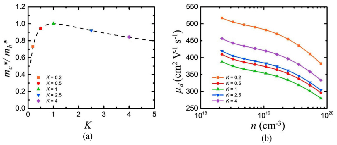
To theoretically demonstrate how changing the shape of Fermi surface pockets affects the thermoelectric performance of p-type Bi-Sb-Te, its electronic transport properties were calculated using varying valence band K with constant band parameters (mb*, Ξ, Nv, and Eg) under the acoustic phonon scattering assumption. The band parameters of Bi-Sb-Te were first obtained via the two-band model while assuming its Fermi surface pockets were spherical (K = 1 for both bands). The K is defined as a ratio of mb* along the longitudinal ellipsoid direction (mb,∥*) to that along the transverse ellipsoid direction (mb,⊥*;).
In terms of K, the degree of decoupling mc* from mb* is determined as below.
When K in Eq. (2) equals to unity, the mc* and mb* are identical, but for K ≠ 1, the mc* becomes lighter than mb* as presented in Fig 1(a) [8]. The solid black line in Fig 1(a) represents mc*/mb* as a function of K. The symbols indicate mc*/mb* for each K in the range from 0.2 to 4. The specific Ks were chosen so that their corresponding mc*/mb* ratios in the valence band were all different. Engineering K to be less than 1 (mb,∥* being heavier than mb,⊥*;) is more effective for decoupling mc* from mb* than changing K to be larger than 1, according to Fig 1(a). In other words, decoupling σ from S becomes possible for a K other than 1.
The μd of Bi-Sb-Te was calculated as a function of n for varying valence band K (0.2, 0.5, 1, 2.5, and 4) to evaluate the effect of engineering K in drift mobility (μd) as shown in Fig 1(b). Commonly, the μd was described to be inversely proportional to mb*5/2 assuming K = 1. However, the μd is more accurately described by a product of mc*-1 and mb*-3/2 for K ≠ 1, as given in Eq. (3).
According to Eq. (4), the μd is inversely proportional to the mc*/mb* ratios, which depend on K (Fig 1(a)). In Fig 1(b), the μd calculated with K = 1 is the lowest for all ranges of n (green triangle and line). In contrast, the μd calculated with K = 0.2 is the highest (orange square and line). Because the mc*/mb* ratio for K = 0.2 (mc*/mb* = 0.73) is smaller than that for K = 1 (mc*/mb* = 1), the μd for K = 0.2 is calculated to be higher than that for K = 1. For other K, the corresponding μd also depends on the reciprocal of the mc*/mb* ratio (Eq. (4)). Therefore, a higher μd is expected with a K that gives a smaller mc*/mb* ratio.
3.2. Effect of varying mc*/mb* on σ via K engineering
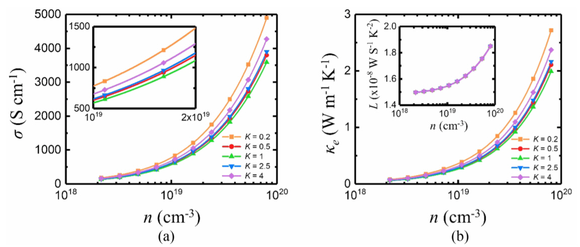
To examine the effect of engineering K on σ, the σ of Bi-Sb-Te was calculated for varying valence band K (0.2 – 4), as shown in Fig 2(a). Because the σ is directly proportional to μd as given below (e is the electric charge),
a similar trend was observed in μd for different K (Fig 1(b)), and this is also expected for σ. According to Fig 2(a), σ for K other than unity were calculated to be higher than that for K = 1. Again, it is the value of mc*/mb* determined from a given K, and not the K itself that is correlated to σ. The mc*/mb* ratios which correspond to K (0.2 – 4) are provided in Table 1 (Eq. (2)).
From Table 1, the K arranged in order of decreasing mc*/mb* are: 1, 0.5, 2.5, 4, and 0.2. The calculated σ is also increased with decreasing mc*/mb* (K: 1 → 0.5 → 2.5 → 4 → 0.2) as shown in Fig 2(a). Engineering K to reduce mc*/mb* was found to be beneficial to increase σ.
A minor difference between σ and μd is that σ only depends on mc*. Because n is directly proportional to mb*3/2, σ becomes inversely proportional to mc* only as below.
In other words, σ is the electronic transport parameter, which can be separated from S most effectively with relevant K engineering.
The effect of varying mc*/mb* (via K engineering) on electronic thermal conductivity (κe) was also studied. The heat-carrying carrier conductions (κe) contribute to the total κ along with heat conductions via lattice vibrations (lattice thermal conductivity, κl) and bipolar conductions (bipolar thermal conductivity, κbp) as in Eq. (7).
Among κl, κe, and κbp, the κe is the most directly related to σ via the Wiedemann-Franz law, as below, where L is the Lorenz number [16].
This is because the L is independent of both mb* and mc*, the κe in Eq. (8) is directly proportional to σ at constant T. Therefore, a higher κe is expected with a K that corresponds to a lower mc*/mb* like σ, but the higher κe decreases zT. Fig 2(b) shows the κe for varying K as a function of n. The κe with K = 0.2 (the lowest mc*/mb*, orange square and line) was calculated to be the largest, and that with K = 1 (the maximum mc*/mb*, green triangle, and line) was calculated to be the smallest. The inset in Fig 2(b) shows the L calculated for varying K as a function of n. Because the L is not a function of mc*, the calculated L are all identical for different K. The discrepancy among κe for different K is calculated to increase at higher n. For the range of n where the thermoelectric performance of most materials is optimized (~1019 cm-3), the increase in κe due to K engineering is negligible. Although decreasing mc*/mb* increases both κe and σ, the improvement in σ outweighs the increase in κe.
3.3. Effect of varying mc*/mb* on S via K engineering
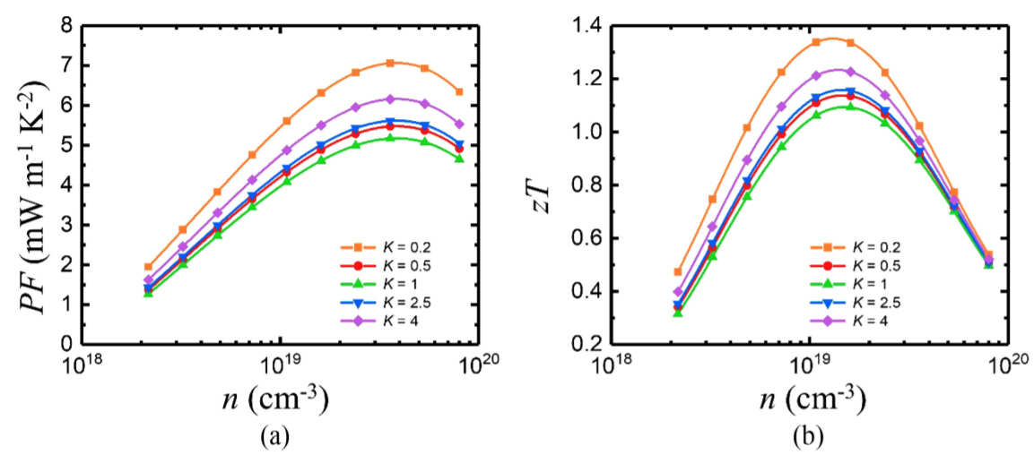
To examine how varying mc*/mb* (via K engineering) affects S, the S of Bi-Sb-Te was calculated for varying valence band K (0.2 – 4) at 300 K, as shown in Fig 3(a). The S for different K are almost identical for n≥ ~5 × 1018 cm-3, but they are different for n < ~5 × 1018 cm-3. Although S calculated from a single band is independent of mc* (but dependent on md* instead), the overall S calculated from two bands does depend on mc* via σ contributions from each band. The overall S is calculated by Eq. (9) below, where Si and σi are the partial contributions from each band (i = VB (valence band), CB (conduction band)).
When σVB and σCB in Eq. (9) are comparable at low n, the difference in σVB due to varying valence band K is well captured in the overall S. For example, the σVB for K = 0.2 is the highest among K in the range from 0.2 to 4 (Fig 2(a)). Hence, the S for K = 0.2 is calculated to be the highest for n < ~5 × 1018 cm-3, as in Fig 3(a) (SVB, SCB, and σCB being constant with respect to K). In Fig 2(a), we simply stated that the overall σ increased because of the decrease in the mc*/mb* ratio. To be more specific, the increase in the overall σ was due to the increase in σVB originating from a decrease in the valence band mc*/mb* ratio (K of the conduction band was fixed). However, once the σVB becomes much greater than σCB at high n, the S in Eq. (9) converges to SVB, as shown below.
Because SVB is independent of mc*, the S is calculated to be approximately invariant with respect to K at n ≥ ~5 × 1018 cm3, as in Fig 3(a). Given that the optimum properties of thermoelectric materials are frequently realized at n ~ 1 × 1019cm-3, it can be concluded that the S is not affected by varying K.
The effect of varying mc*/mb* (via K engineering) on κbp was also examined. Unlike κe, both Si and σi (i = VB, CB) are required to calculate κbp, as shown below.
In Eq. (11), the SVB and SCB are independent of varying K, as they do not depend on mc*. And because we assume that the K of the conduction band is unity for simplicity, only the σVB is changed with varying K. Therefore, it is expected that the κbp with a low mc*/mb* will be high because of high σVB, as in the case of S. However as calculated in Fig 3(b), the discrepancy in κbp due to different K is negligible for all n. Hence, varying K does not affect κbp.
3.4. Effect of varying mc*/mb* on power factor via K engineering
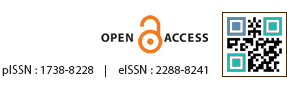
To demonstrate the effect of varying mc*/mb* (via K engineering) on the power factor, the power factor of Bi-Sb-Te was calculated for varying valence band K (0.2 – 4) at 300 K as shown in Fig 4(a). Since suppressing mc*/mb* is beneficial to σ (Fig 2(a)), while causing a negligible change in S (Fig 3(a)), an improvement in the power factor is expected. According to Fig 4(a), the highest power factor was calculated for the K = 0.2 (orange square and line), which corresponds to the lowest mc*/mb* (Table 1), and the lowest power factor was calculated for K = 1 (green triangle and line) which corresponds to the maximum mc*/mb*. The calculated power factor increased with decreasing mc*/mb* (K: 1 → 0.5 → 2.5 → 4 → 0.2), as observed in σ in Fig 2(a). Therefore, engineering K to be other than unity will always improve the power factor.
Lastly, to investigate the effect of varying mc*/mb* (via K engineering) on zT, the zT of Bi-Sb-Te was calculated for varying valence band K (0.2 – 4) at 300 K as shown in Fig 4(b). For the zT calculation, κl is required in addition to the κe and κbp calculated in Fig 2(b) and 3(b), respectively. Because the κl cannot be calculated using the two-band model, the experimental κl of a state-of-the-art Bi-Sb-Te ingot was adopted from the literature (κl = 0.8 W/m-K at 300 K) [9]. The highest zT was calculated for K = 0.2 for all n, as shown in Fig 4(b). Its optimum zT was achieved near n ~ 1019 cm-3. The sharp decrease in zT for n > 1019 cm-3 is attributed to the increasing κe and κbp at high n. This confirms that engineering K to decrease mc*/mb* is another effective approach to improve zT.
Engineering K is another effective band engineering approach to improve the power factor of thermoelectric materials. Making K other than unity decouples mc* from mb*, which enables us to break the trade-off between S and σ. As mc*/mb* decreases, σ is improved without deteriorating S. Although κe is also increased with decreasing mc*/mb*, the κe increase is negligible compared to the σ increase. Therefore, zT improvement is guaranteed if the mc*/mb* is reduced by engineering K.
We assumed that the K of both the valence and conduction bands were unity when obtaining the band parameters of the state-of-the-art Bi-Sb-Te ingot from the two-band model fitting. However, it has been reported that the valence band K of Bi-Sb-Te was optically determined to be approximately 2 [17]. Consequently, the determined band parameters of Bi-Sb-Te (mb*, Ξ) with K = 1 can be marginally different from what they should be (with K = 2). The discrepancy between the fitted Ξ and the actual Ξ will be higher than that expected between the fitted and actual mb* because K only affects mc*-related parameters. Nonetheless, the fact that engineering K improves power factor remains intact because the beneficial effect of decreasing mc*/mb* on power factor applies to any set of band parameters.
Both decreasing mc*/mb* by engineering K and decreasing Ξ have similar impacts on μd as the μd is inversely proportional to the product of Ξ2, mc* and mb*3/2. In addition, because S is independent of Ξ, the effect of suppressing Ξ on electronic transport properties is almost identical to the effect of engineering K on electronic transport properties. Therefore, an additional optical study that measures mb* at different principal axes is required to confirm that an improvement in power factor originates from K engineering.
No experimental approach to engineer only K has been suggested yet. Although alloying is known to alter K, it also changes other band parameters at the same time, making the evaluation of the effect of K change difficult [17]. As an alternative, materials with innately low mc*/mb* have been theoretically sought as potential candidates for new high-performance thermoelectric materials [18].
Although the effect of engineering K was investigated using narrow band gap Bi-Sb-Te, its effect will be even greater for large band gap materials since the potential increase in κbp due to K engineering will be minimized because of their substantially low κbp [19]. Moreover, since we know that K other than unity can significantly alter the electronic transport properties of thermoelectric materials, accurate K input (obtained via measurements or simulations) is important to accurately determine materials’ band parameters via band modeling.
4. Conclusions
A new band engineering approach that by-passes the trade-off between S and σ has been suggested. Engineering the shape of Fermi surface pockets (K, non-parabolicity factor) to be ellipsoidal was found to decouple conductivity effective mass (mc*) from the band mass of a single Fermi pocket (mb*). When K is engineered to lower the mc*/mb* ratio, the σ is calculated to increase while S remains constant. It was calculated that the thermoelectric figure-of-merit (zT) of a Bi-Sb-Te ingot can be improved to higher than 1.3 if the nonparabolicity factor is engineered to be 0.2. Although alloying is known to change K, it also simultaneously alters other band parameters. However, it is suspected that alloying, combined with carefully designed doping, might only change K so that it improves the power factor of materials effectively.