


1. Introduction
Ga2O3 is one of the most promising candidates for high power electronic devices due to its large bandgap energy and high breakdown voltage characteristics. Extensive research work has recently been conducted to implement Ga2O3-based power electronic devices with higher critical field strength and efficiency compared to their GaN and SiC counterparts [1-3]. As a newly emerging ultra-wide bandgap semiconductor, the most stable β-phase among the five Ga2O3 polymorphs [4-6] is preferred, and most of the recent research has been focused on β-Ga2O3 field effect transistors (MOSFETs and MESFETs) and Schottky barrier diodes [7-10].
More recently, there has been increasing interest in α-phase Ga2O3, given its several advantages over β-Ga2O3. α-Ga2O3 has a larger bandgap (~5.3 eV) and higher Baliga’s figure-ofmerit (FOM) compared to β-Ga2O3 [11,12]. It has the same corundum crystal structure as a sapphire substrate with the smallest lattice mismatch among the polymorphs of Ga2O3, and this allows high quality, large area epitaxial growth using various growth techniques such as Halide Vapor Phase Epitaxy (HVPE), Mist Chemical Vapor Deposition (mist-CVD), and Molecular Beam Epitaxy (MBE) [13-15]. In addition, tuning of the bandgap energy from ~3.7 to ~8.75 eV is possible through alloying with α-In2O3 and α-Al2O3 [16,17]. For example, a α-Ga2O3 Schottky barrier diode showed a lower on-resistance of 0.1 mΩ·cm2 compared a β-Ga2O3 Schottky rectifier [18].
When fabricating α-Ga2O3-based microelectronic devices such as MOSFETs, Schottky barrier diodes, UV detectors, and UV-LEDs, a patterning process that accurately transfers various features into the α-Ga2O3 layer is essential. The pattern transfer can be carried out by either wet etching or dry etching. There have been some reports on the wet etching of β-Ga2O3 [19-23], but it is very difficult to produce practical etch rates with conventional wet etching at low temperature, because of the high chemical inertness of Ga2O3. Moreover, the isotropic nature of wet etching makes it incapable of performing high resolution pattern transfers of sub-micron device features [24,25]. Dry etching techniques utilizing a high density plasma source, such as inductively coupled plasma (ICP) and electron cyclotron resonance (ECR), have been shown to produce higher etch rates for GaN and SiC compared to conventional reactive ion etching (RIE) and chemically-assisted ion beam etching (CAIBE) [26-30]. In addition, the ion-induced damage can be minimized because of the ability to control ion flux and ion energy separately. Therefore, high density plasma etch techniques are the preferred patterning technique for α-Ga2O3-based microelectronic devices. However, there have been only a few reports on the high density plasma etching of α-Ga2O3 epitaxy film [31].
In this work, we report a parametric study on the etch characteristics of α-Ga2O3 epitaxy film grown on sapphire in two fluorine-based (CF4/Ar and SF6/Ar) inductively coupled plasmas. The effects of plasma composition, ICP source power, rf chuck power and process pressure on the etch rate, surface morphology and etch anisotropy were studied.
2. Experimental
α-Ga2O3 epitaxy films were grown on 2 inch diameter c-axis sapphire substrates using the horizontal halide vapor phase epitaxy (HVPE) method. During the growth process, Ga metal, HCl and O2 gases were used as precursors and the substrate temperature was maintained at 470 °C, and the typical thickness of the grown α-Ga2O3 epitaxy films were ~1 μm [32,33]. The surface of the grown α-Ga2O3 epitaxy film was chemically cleaned and then, the samples were patterned with AZ5214 photoresist and Nickel. The etching of the α-Ga2O3 epitaxy film was performed in a planar type inductively coupled plasma (ICP) source operating at 13.56 MHz and power up to 1000W, and the samples were thermally bonded to a Si carrier wafer that was mechanically clamped to a He backside-cooled, rf-powered (13.56 MHz, up to 450W) chuck. CF4/Ar and SF6/Ar ICP discharges with a total gas load of 15 standard cubic centimeters per minute (sccm) were employed to etch the α-Ga2O3, and the process pressure was varied from 2-20 mTorr during etching. After removal of the mask layer, the etch rate, surface morphology and anisotropy of the etched features were characterized by stylus profilometry, tapping mode atomic force microscopy (AFM) and field-emission scanning electron microscopy (FE-SEM), respectively.
3. Results and Discussion
Figure 1 shows the plasma composition dependence of the α-Ga2O3 etch rate in CF4/Ar and SF6/Ar ICP discharges under fixed ICP source power (500W), rf chuck power (150W) and pressure (2 mTorr) conditions. In the SF6/Ar discharges, the etch rate initially increases as the SF6 content increases due to the increase in reactive fluorine radical density in the plasma. After reaching a maximum value of ~392.8 Å/min at 86.7% SF6 content, the etch rate decreases in pure SF6 discharge due to the reduced ion-assisted removal of the GaFx etch products (presumably GaF3 ; b.p. 1000 °C) formed on the surface. In the case of CF4/Ar discharges, as the CF4 content increased to 13.3 %, the α-Ga2O3 etch rate rapidly increased by a factor of ~4 compared to the pure Ar discharge. This is attributed to the formation of GaFx etch products enhanced by the CF4 addition and balanced with subsequent ion-assisted desorption. However, further increases in the CF4 content led to a reduction in the etch rate, most likely due to the build-up of a fluorinated selvedge layer with low volatility on the surface.
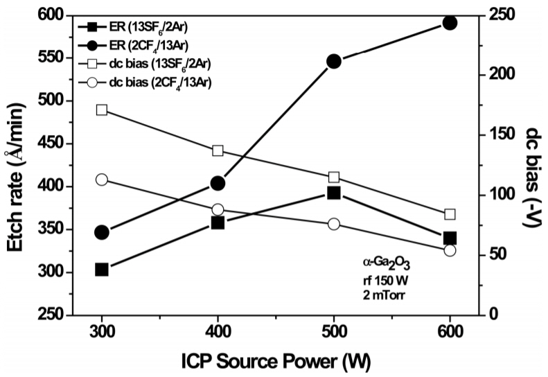
Figure 2 shows the effect of ICP source power on the α-Ga2O3 etch rate in the 2CF4/13Ar and 13SF6/2Ar discharges, which produced the highest etch rates among the composition conditions presented in Figure 1. In the 2CF4/13Ar discharges, the etch rate showed a strong dependence on the source power and higher etch rates were obtained compared to the 13SF6/2Ar discharges. The α-Ga2O3 etch rate continuously increased as the source power increased, due to the increased reactive fluorine radical density and ion flux in the discharge. A maximum etch rate of ~592 Å/min was obtained at 600W source power. A similar trend was observed in the 13SF6/2Ar discharges up to a source power of 500W. The decrease in the etch rate at 600W source power is most likely related to a decrease in ion energy caused by an increase in the source power.
The α-Ga2O3 etch rate as a function of the rf chuck power in the 2CF4/13Ar and 13SF6/2Ar discharges is shown in Figure 3. During etching, the ICP source power and pressure were maintained at 500W and 2 mTorr, respectively. In both the 2CF4/13Ar and 13SF6/2Ar discharges, the etch rate monotonically increased as the rf chuck power increased, indicating the etch reaction under these conditions is dominated by the physical component of the etching. Increasing the rf chuck power increases the energy of the ions in the discharges (Ar+ and CF3+ in the 2CF4/13Ar, and Ar+ and SF5+in the 13SF6/2Ar, respectively) [34-36] and improves the ionassisted removal of nonvolatile GaFx etch products. Then this leads to an increase in the etch rate. Maximum etch rates of ~855 Å/min and ~548.3 Å/min were obtained with a moderate rf chuck power (250 W) in the 2CF4/13Ar and 13SF6/2Ar discharges, respectively.
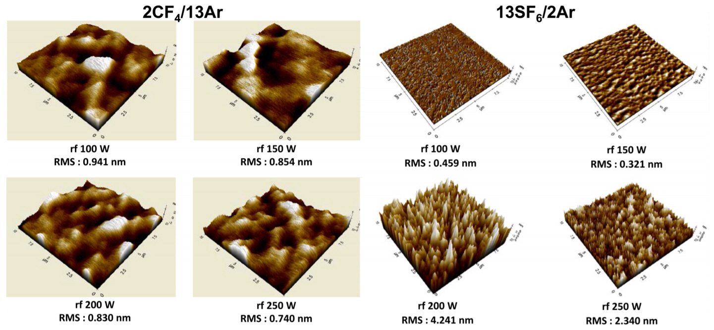
Figure 4 shows the AFM surface scan images of the α-Ga2O3 epitaxy films etched in the 2CF4/13Ar and 13SF6/2Ar discharges with variation of rf chuck power at a fixed source power (500 W) and pressure (2 mTorr). The determined normalized roughness is presented in Figure 5. Etch depth in each sample was maintained at ~2000 Å and the root-meansquare (RMS) roughness of the unetched α-Ga2O3 control sample was ~0.68 nm. The α-Ga2O3 samples etched in the 2CF4/13Ar discharges show almost the same surface roughness as the unetched control sample (normalized roughness in the range of 1.08-1.38) over the entire rf chuck power conditions examined. This is a typical feature of a physically-dominated etch process where the angular dependence of the ion milling removes sharp surface features faster [37].
For the 13SF6/2Ar discharge, the α-Ga2O3 samples etched at a low rf chuck power of 150 W or less showed smoother surface morphology than the unetched control sample, while significant surface roughening was observed at rf chuck powers above 200 W, most likely due to the inhomogeneous removal of GaFx etch products or surface atoms by enhanced ion bombardment.
The effect of process pressure on the α-Ga2O3 etch rate in the 2CF4/13Ar discharge is shown in Figure 6. As the process pressure increases, the etch rate continues to decrease due to the reduced physical contribution to the etching. This is because the increase in the process pressure reduces the mean-free-path of ions in the discharge and increases the energy loss of ions impinging on the surface.
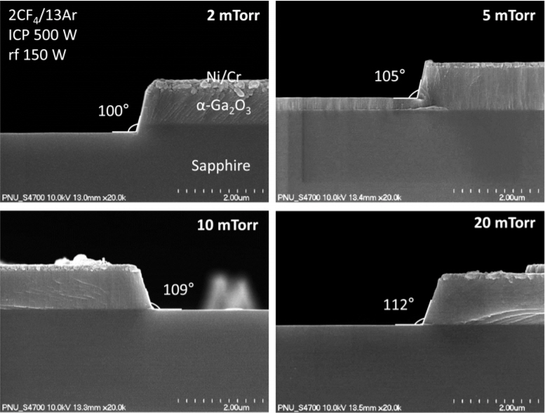
Figure 7 shows the SEM cross-sectional images of the features etched into the α-Ga2O3 layer under the same conditions presented in Fig 6. Please note that the Ni mask layer is still in place. In the case of the feature etched under the lowest pressure condition of 2 mTorr, it can be seen that a highly anisotropic pattern transfer with a quite vertical sidewall (~100 °) was achieved due to the ion-assisted nature of the etching. But as the process pressure increased, the frequency of normal incidence of ions was reduced due to the increased collisions with other ions or neutrals in the discharge, resulting in an increased off-angle from the vertical.
4. Summary and Conclusions
High density plasma etching of α-Ga2O3 epitaxy film was performed in CF4/Ar and SF6/Ar inductively coupled plasmas and the effect of plasma composition, ICP source power, rf chuck power and process pressure on the etch rate, surface morphology and etch profile was examined. In the CF4/Ar discharges with low CF4 content, a significant increase in the etch rate was observed due to the synergetic effect between the physical and chemical component of the etching. However, the etch rate generally increased with increasing SF6 content in the SF6/Ar. The etch rate showed a stronger dependence on the source power and rf chuck power in the 2CF4/13Ar discharge compared to the 13SF6/2Ar discharge. The 2CF4/13Ar discharge produced higher etch rates under all conditions examined, and maximum etch rates of ~855 Å/min and ~548.3 Å/min were obtained in the 2CF4/13Ar and 13SF6/2Ar discharges, respectively at 500 W source power, 250 W rf chuck power, and 2 mTorr pressure. The α-Ga2O3 surfaces etched either in the 2CF4/13Ar or low rf chuck powered (less than 150W) 13SF6/2Ar discharge showed a smooth morphology. Highly anisotropic pattern transfer was performed in the 2CF4/13Ar discharge with low pressure (2 mTorr) due to the ion-assisted nature of the etching, and the etch rate and etch anisotropy were reduced as process pressure increased. The results of this work show that fluorine-based ICP etching would be a reasonable choice for fabricating a α-Ga2O3 device structure with a smooth surface morphology.