


1. INTRODUCTION
Electrical steels are used as the core for electric motors in hybrid vehicles or in power or delivery transformers as they increase the efficiency of these devices. Because of these applications, electrical steels are considered one of the high-value steel materials for the future. The performance of electromagnetic devices is directly related to magnetic properties including hysteresis and core loss, which depends on the magnetic domain structures. Recent developments of electrical steels have improved these performances. At the same time, there has been little effort to develop new evaluation techniques for the performance of electrical steel.
Various techniques that can visualize the magnetic domain are briefly described in Ref. [1]. The magnetic powder method, called the Bitter method [2], which is a classical method, visualizes the magnetic domain by detecting the interaction of ferrite magnetic powders with stray fields occurring perpendicular to the sample surface. The powders agglomerate at positions of maximum magnetic flux, in particular domain walls, and the domain visualized by the optical microscope is limited to the domain on the top surface of sample.
Magneto-optical microscopy techniques [3,4], magnetooptical Kerr effect (MOKE) or magneto-optical Faraday effect (MOFE), visualize the domain at the sample surface by detecting the rotation of linearly polarized light reflected or transmitted from the magnetized surface respectively. The methods are light-based techniques so the acquired magnetic domain is only for the sample depth of tens of nanometers, and especially for MOKE the sample should be carefully polished and annealed to remove the insulating coating surface and to get strain free to minimize the deformation of magnetic domain.
Electron microscopy techniques (Lorentz microscopy [5] and scanning electron microscopy (SEM) [6,7]) visualize the magnetic domain with resolution down to micrometer scale. The former, based on the Lorentz force, maps the magnetic domain by detecting the deflection of electrons as they pass through the magnetic induction field of the sample. The latter detects reemitted electrons from the sample, and it reveals the magnetic stray fields outside the sample by detecting secondary electrons of low energy for the type I and the magnetic field inside the sample by detecting back-scattered electrons of high energy for the type II. The SEM with polarization analysis (SEMPA) [8] is another technique which detects the spin polarization of secondary electrons directly related to the magnetization of sample. Though electron microscopy enables observing the magnetic domain for thicker samples with a depth of several micrometers, it is still surface-sensitive, which means it is difficult to measure bulk samples, and cannot be used with an external magnetic field which disturbs the image contrast of the magnetic domain.
Magnetic force microscopy (MFM) [9] is a local probe technique for visualizing the magnetic domain with resolution down to about several tens of nanometers. It simultaneously visualizes topographic and magnetic images by detecting the magnetic interaction between the sharp magnetized tip and the sample surface. However, the technique allows only a few special samples and conditions, and suffers from the disturbance on sample magnetization due to the ferromagnetic probe tip.
Intensive studies on the visualization of magnetic domain structures have been carried out using the above-mentioned techniques to understand physical characteristics of magnetic domains. Magnetic domain imaging has been applied to investigate not only the grain structures related to the wall movement of magnetic domains on the effect of precipitates [10, 11] but the characterizations of electrical steel sheet with respect to the mechanical stress generated by a compression [12], a tension [13], a cutting [14], and a coating [15]. Furthermore, the dynamic domain imaging at power frequencies have been investigated [16,17]. However, since the above-mentioned techniques are surface-sensitive the results strongly depends on the thickness and the preparation state of the sample.
In contrast, neutron imaging holds high potential as a non-destructive method that can visualize magnetic domain structures of the bulk sample owing to the long penetration depth of neutrons, i.e. several centimeters. Since the neutron possess a magnetic moment, the magnetic structure of a sample be visualized by detecting the change in the magnetic moment. There are several techniques to visualize magnetic domain structures using neutrons; polarized neutron imaging [18], dark-field imaging of neutron grating interferometry [19-21], and neutron topography [22]. Neutron grating interferometry visualizes the magnetic domain structure of magnetic materials by providing the dark-field image (DFI) based on small angle neutron scattering (SANS) and has been actively studied on the electrical steel sheet [23-27].
In this paper, we describe high-resolution dark-field imaging for visualizing the magnetic domains of electrical steel sheets using neutron grating interferometry. The neutron grating interferometer with the camera-based high-resolution system produces the high-resolution DFI, and it reveals the magnetic domains inside the electrical steel sheets. The electrical steel sheets were also measured by the Bitter method and the classical magnetic domain results were compared with the DFI results.
2. EXPERIMENTAL PROCEDURES
One can describe how the neutron interacts with a material according to a refractive index, n = 1 –δ+iβ, which consists of the real part δ related to a nuclear potential and the imaginary part β related to absorption and incoherent scattering. In the case of a magnetic material, the neutron interaction is additionally affected by the magnetic field of the material, and the refractive index of neutron becomes n = 1 - δnuc - δmag + iβ, where a nuclear contribution δnuc and a magnetic contribution δmag, in the interaction of the magnetic material [28].
It is well known that electrical steel consists of magnetic domains, which is the region of equally magnetic moment pointing with the saturated value of magnetization. The typical magnetic domain of electrical steel can be classified by the basic domain and the supplementary domain. The basic domain consists of wide domain structures having parallel and antiparallel magnetization vectors to the easy direction. The supplementary domain consists of shallow domain structures which have a misorientation angle of less than a few degrees with respect to the easy axis. These shallow structures include internal and transversely magnetized domains and surface lancets, are superimposed on the basic domain to reduce the stray field energy caused by the misorientation and are mainly generated at the grains of large misorientation angle and the grain boundaries. The magnetic domain has a boundary line, called a domain wall, between adjacent magnetic domains. Thereby, the neutron is refracted as it passes through the domain wall. The refraction of the neutron at the domain wall can be regarded as SANS, and hence the magnetic domain structure of electric steel can be resolved by a neutron grating interferometer [28]. In this experiment, the magnetic domain, grain-oriented electrical steel sheets (25 × 40 × 0.23 mm3) which are laser-irradiated in distances of 5 mm and 2 mm perpendicularly to the direction of domain walls, was observed by the neutron grating interferometer.
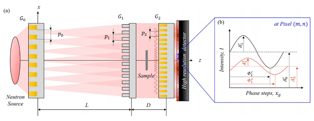
The neutron grating interferometer was a Talbot-Lau interferometer (TLI) as shown in Fig 1. The TLI consists of a source grating (G0), a phase grating (G1), and an analyzer grating (G2), and they have a line structure of micrometer scale. The G0 has a neutron absorbing material such as a gadolinium (Gd) or gadolinium oxysulfide (Gadox). It is positioned in front of the neutron source and generates several neutron beams to achieve a spatial coherence for the initial condition of interference. The G1 has a neutron phase shifting material such as silicon. It induces a phase modulation of the neutron beam and creates the interference pattern, called a Talbot pattern, which is generated behind of G1. The Talbot pattern is an intensity structure along the beam path, and it includes a periodic intensity structure, called a self-image, as to the detector plane at the Talbot distance. The G2, another neutron absorbing grating, located at the Talbot distance in front of the detector creates a sufficiently wide periodic intensity structure, called a Moiré pattern, to resolve the self-image of several micrometers, allowing to be analyzed by the detector pixel of tens of micrometers.
The Moiré pattern is recorded by detector pixels using the phase stepping method in which one of the gratings moves several fractional intervals of its period in the perpendicular direction to the grating structure, and hence a stack of images at different phase steps are obtained. For the equivalent pixel position of the image stack, the intensity of the Moiré pattern is recorded as a sinusoidal intensity oscillation as to phase steps and is schematically shown in Fig.1 (b).
The sample deforms the intensity structure of Talbot (and hence Moiré) pattern (sinusoidal red line in Fig 1a). The Moiré pattern is analyzed in each detector pixel (m,n) along phase steps xg is expressed in a Fourier series by [28]
, where Ai is the amplitude coefficient, Φi is the phase coefficient, k = 2π pi is the wave number, pi is the period of G1, and xg is the fractional interval of pi (i.e. the size of phase step). The sinusoidal intensity oscillation is characterized by coefficients of the offset A0, the amplitude A1, and the phase Φ1, which can be extracted by Fourier analysis.
The DFI that reveals the magnetic domain of electrical steel sheet is obtained by
where V is the visibility, and Ai is the extracted Fourier coefficients of ith amplitude coefficient in Eq. (1). Here, we denote indices in Eq. (2) for without sample (reference) and with sample by superscripts r and s respectively. The visibility is the intensity modulation of the Moiré fringe, which is the ratio of 0th and 1st amplitude coefficients, and the DFI is the ratio of visibility without sample (Vr) and with sample (Vs).
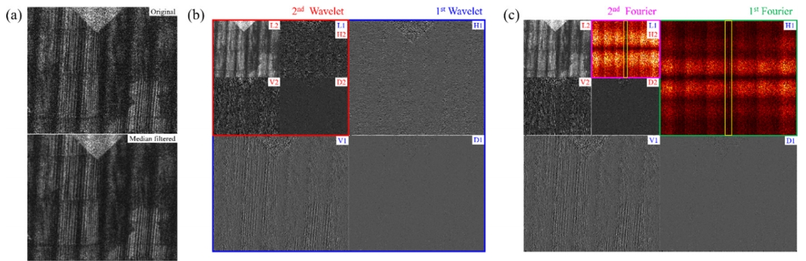
The sCMOS camera has amplifiers on each individual photosensor or each row of the photosensor, and the row of pixels can be readout the signal in parallel. The addressed readout feature results in a stripe artifact in the image and can degrade the image quality, especially in the image acquisition of line arrays such as the magnetic domain of electrical steel sheet. To remove the stripe artifact, the camera was installed as perpendicularly to the direction of domain wall and the combined wavelet-Fourier filtering was processed.
The combined wavelet-Fourier filtering process [29] is the consecution of the selective Fourier filtering for the aimed structure resulted by the wavelet filtering. The original image is initially filtered by the median filter to reduce non-statistical noises before the 1st wavelet filtering as show in Fig 2 (a). The wavelet filtering separates the structural information of the image in the low frequency, horizontal, vertical and diagonal detail bands corresponding to L1, H1, V1, and D1 respectively as shown in Fig 2 (b). In the experiment, the stripe artifact of the amplifiers is perpendicular to the domain wall, so the information of those structures is decomposed into vertical and horizontal detail bands respectively. Subsequently, the structural information of the stripe artifact is processed by Fourier filtering the frequency region for amplifier arrays, indicated by the vertical yellow line box in H1 in Fig 2 (c), by multiplication of a Gaussian window function. The former filtering processes are additionally conducted for the low frequency detail band of lower classes of wavelet filtering to obtain further improved image result within the final image that is not distorted. Figure 2 shows the combined wavelet-Fourier filtering of decomposition levels of two. The filtering parameters are the specific type of wavelet filtering, the standard deviation of Gaussian function, and the number of class levels which is the repetition of combined wavelet-Fourier filtering. In this work, the type of wavelet filtering was set Daubechies Level 1, the standard deviation of Gaussian function was 0.2, and the decomposition level was repeated 5 times.
The measurements were performed at the cold neutron beamline NG6 of the NIST Center of Neutron Research (NCNR) [30] and the details of TLI are shown in Table 1. It was operated in polychromatic beam with wavelengths above 0.4 nm due to a cut off by a beryllium filter of 5 cm. The beam-defining aperture diameter of the neutron source was 13 mm. The G1 produces the phase shift of π at the effective wavelength of 4.4 Å. The detector was an Andor sCMOS camera [31] with Nikon lens of 105 mm [31] with reproduction ratio of 1, and the image array was 2560 × 2160 pixels with effective pixel pitch of 6.5 μm. The exposure time for each image was 180 s, and 15 images were merged by median filter to reduce non-statistical noise. The scintillator was a Gadox screen of 20 μm in height. The phase stepping consisted of 8 steps of G0 driven in direction of x-axis and the electrical steel sheets were positioned 15 mm from G1.
The electrical steel sheets were observed by the Bitter method and compared with the DFI. The magnetic domain viewer (Model No. MI-19-2, Sensorpia) was used and the domain structure was captured by an optical microscope.
3. RESULTS AND DISCUSSION
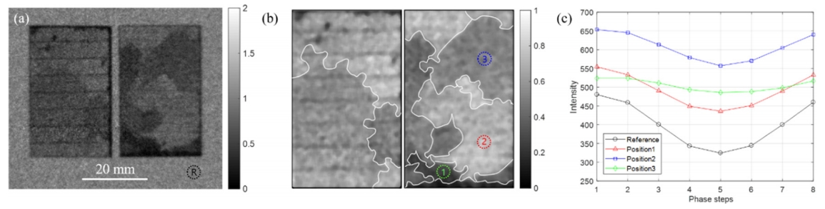
An example DFI of electrical steel sheets measured by a lower spatial resolution TLI system [32] is shown in Fig 3 (a). The electrical steel sheets were irradiated with a laser for two different the laser-irradiated distances of 5 mm and 2 mm. The DFI shows the magnetic domain consisting of several grains with each different contrast as shown in Fig 3 (b), which is a median-filtered image with the filter size of 10×10 pixles for cropped regions of electrical steel sheets in Fig 3 (a). The contrast of each grain in the DFI results from the in SANS of each grain and differs because of distribution of crystallographic orientations.
Figure 3 (c) shows intensity oscillations of the Moiré pattern at the sample and reference reagions shown in Fig 3 (a) and (b). It shows the measured intensity varying by the phase stepping, and the visibilities in the sample region is lower compared with the visibility of the reference region due to the higher dark-field contrast, which means more small angle scattering occurs in the sample region. The reference region has a visibility of 15%.
The DFI also shows laser-irradiated lines as shown in Fig 3 (a). The dark-field contrast of laser-irradiated lines, which are higher than the contrast of the neighboring region, means more SANS originates from here, and it is due to the supplementary domains created by the laser-irradiation [23]. In general, it is well known that the supplementary domains observed near laser-irradiated lines are attributed to compressive stress in the vicinity of laser-irradiated line [33]. This compressive stress results from the thermal shock at the fast heated and cooled zones due to the laser-irradiation [34,35]. That is, since the region where compressive stress appears makes magnetoelastic energy increase, the supplementary domains are stabilized in the laser-irradiated lines, thereby generating complex domain structure which has a large number of domains in the vicinity of laser-irradiated line [34]. The complex domain depends on the laser energy, and the laser-irradiation with higher energy creates a more complex domain with many domains [36]. Therefore, the contrast of laser-irradiated lines of the left sheet is higher than that the right sheet, which means the left sheet is relatively strongly laser-irradiated. Furthermore, the SANS which is generated at the laser-irradiated edges like as that there is a higher contrast at the edges of the electrical steel sheets contributes to the additional dark-field contrast of laser-irradiated lines.
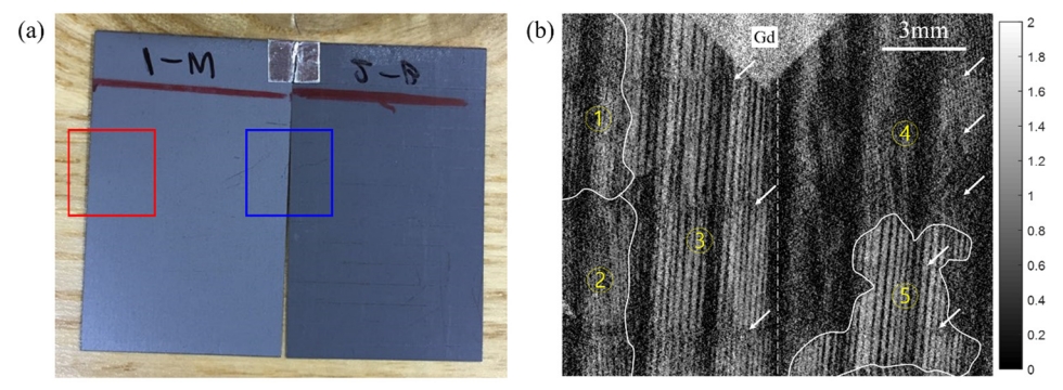
An optical photograph of electrical steel sheets and the corresponding high-resolution DFI in the region of interest (ROI) indicated by the blue box are shown in Fig 4. In both the photograph and the DFI, the electrical steel sheet with the laser-irradiated distance of 5 mm is shown on the right and the sheet of 2 mm is on the left. In Fig 4b the laser-irradiated lines of both electrical steel sheets are marked by arrows. In the high-resolution DFI, the degradation of visibility represents the domain wall directly and the domain wall appears as the dark stripe itself, and hence the grain boundaries are estimated by the direction and density of domain walls.
The high-resolution DFI shows refined basic domains after the laser-irradiation since it directly displays domain walls at grains. For the electrical steel sheet of the laser-irradiated distance of 5 mm, the ROI displays three grains of refined basic domains, and grains ① and ② show more refined domains than the grain ③. Similarly, for the electrical steel sheet of 2 mm distance, the grain ④ shows more refined domains than the grain ⑤. The number of domain walls at grains ① to ⑤ are 18, 20, 12, 25, and 12 respectively for the length bar of 3 mm. It isn’t exactly comparable to the width of domain wall between grains, but quantitatively, the widths of domain wall at grains ① to ⑤ are 0.17 mm, 0.15 mm, 0.25 mm, 0.12 mm, and 0.25 mm respectively.
In Fig 4 (b), for highly refined grains, the grain ④ in the electrical steel sheet with the laser-irradiated lines of 2 mm, seem to have relatively higher contrast compared with grains ① and ② in the sheet with the laser-irradiated lines of 5 mm. These fine grains result in the significant reduction of visibility due to the relatively large SANS. There are two possibilities for the phenomenon. It is well known that the refinement of the basic domain structure is due to tensile stress between laser-irradiated lines to decrease the stray field energy [33], and it is related to the conditional parameters of laser-irradiation such as the laser energy and the laser-irradiated distance [35]. As mentioned above, the laser energy is related to complex domains due to supplementary domains in the vicinity of laser-irradiated line. In addition, the width of basic domain is refined when the laser energy decreases. Hence, grain ④ shows more refined basic domains than grains ① and ②, and it results higher contrast by corresponding density of domain walls. The other possibility is the existence of supplementary domains. A narrower laser-irradiated distance induces higher compressive stress in a unit area on the sheet [36] and forms supplementary domains which are stabilized by the compressive stress. In this case, the dark-field contrast of domain walls related with the supplementary domains in the grain ④ is relatively higher than that of grains ① and ②. As shown in Fig 4 (b), for this reason, the electrical steel sheet with the laser-irradiated lines of 2 mm shows much dark area compared with the sheet of 5 mm.
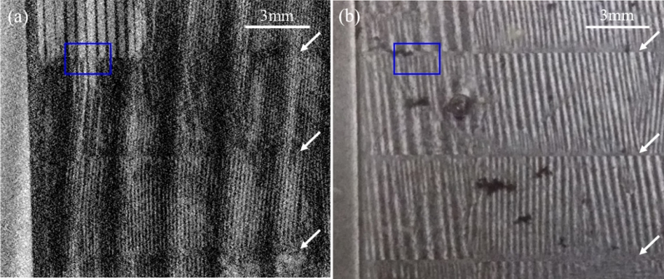
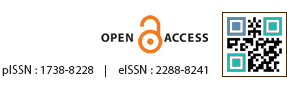
The Fig 5 shows the result using high-resolution DFI and Bitter method of electrical steel sheet with a laser-irradiated distance of 5 mm for the red box in Fig 4 (a). The DFI clearly shows narrower domain walls than the image of the Bitter method. It is because the magnetic powder agglomerates over the magnetic domain walls on the top of the electrical steel sheet [38] while the neutron can penetrate into the electrical steel sheet and directly interact with the inner domain walls. Hence, as shown in the blue box in Fig 5, the DFI shows the narrow domain walls without discontinuity in respect of the laser-irradiated lines (arrows in Fig 5), while the image of the Bitter method shows clearly wide and discontinuous domain walls. Therefore, the DFI allows more accurate magnetic domain observation to understand physical characteristics by showing magnetic domains regardless of the laser-irradiated lines shown as an artificial grain boundary when observed by the Bitter method.
Both methods have interruption elements for visualizing the magnetic domain. The magnetic powder creates the agglomeration across the domain walls as shown in Fig 5 (b). In Fig 5 (a), the wide vertical dark periodic lines over the entire images based on the mismatch of the Moiré pattern results in the interruption of the magnetic domain visualization and makes difficult to estimate grain boundaries in this image. However, this systematic can be removed by the precise grating alignment or translating the phase grating instead of the source grating.
4. CONCLUSION
The neutron TLI is used for visualizing the magnetic domain of electric steel sheets. The high-resolution DFI shows the magnetic domain resulted by the degradation of visibility based on the SANS at domain walls. The magnetic domain observed by DFI shows the grains of the refined basic domains and the supplementary domains superimposed on the basic domain. The DFI directly visualizes domain walls inside electrical steel sheets compared with the Bitter method, so more detailed magnetic domain images have been acquired and the domain wall with a width of down to 0.12 mm could be directly visualized. In addition, the magnetic domain image that are not influenced by the laser-irradiated lines has been acquired as well. The DFI for visualizing the magnetic domains is expected to have a great potential because in-situ measurement of domains is possible as to a magnetic field and the mechanical stresses such as tension, compression, heat, and corrosion through further studies.