


1. INTRODUCTION
The increasing use of transparent conducting oxide (TCO) thin films for various display devices is stimulating the development of inexpensive TCO films that simultaneously have high optical transmittance and low resistivity [1]. Recently, gallium or aluminum doped zinc oxide (ZnO) films have attracted attention, because of their appropriate visible transmittance, low resistivity, and relatively low cost compared to conventional Sn-doped In2O3 (ITO) thin films [2].
It is well known that most metal-doped ZnO films require high substrate temperatures (≥ 300 °C) to increase the electrical conductivity and visible transmittance [3]. However, for flexible, durable, and lightweight display systems, high substrate temperatures are undesirable, because of the low thermal resistivity of plastic substrates. Accordingly, many studies [4-6] have focused on room temperature technologies that can ensure both high optical transmittance and low resistivity in TCO films, without deformation of the flexible polymer substrates.
In this study, we deposited ZnO 50 nm/Ag 10 nm/SnO2 50 nm/(ZAS) tri-layer films using radio frequency (RF) and direct current (DC) magnetron sputtering. Then we electron beam-irradiated the films to investigate the effect of electron irradiation on their electrical and optical properties, using x-ray diffractometer (XRD), atomic force microscopy (AFM), and UV-visible (UV-Vis) spectrophotometry, respectively.
2. EXPERIMENTAL PROCEDURES
Figure 1 shows the RF and DC magnetron sputter system with an electron irradiation (INFO-RFE-60G, Infovion) that was used to deposit the ZnO 50 nm / Ag 10 nm / SnO2 50 nm (ZAS) tri-layer films at room temperature. We used slide glass (size: 25 × 25 mm, thickness: 1.0 mm, Corning 2948) as the substrate. The distance from the target to the substrate was kept at 60 mm.
Prior to deposition, we evacuated the chamber to 5.0 × 10⁻⁷ Torr, and then injected inert argon (Ar) gas at a constant flow rate of 10 sccm to maintain a deposition pressure at 1.0 × 10⁻³ Torr for all depositions. During deposition, both the ZnO and SnO2 targets were biased RF 2.5 W/cm2, while the Ag target was DC 2.0 W/cm2. For ZAS films deposited at room temperature, the substrate temperature was increased from 30 to 60 °C.
After deposition, we biased an electrical power of 200W on an RF (13.56MHz) antenna in an electron beam source and varied the electron irradiation energy at 300, 600, and 900 eV in a low vacuum of 1 × 10⁻⁵ Torr (Ar atmosphere).
We investigated the crystallinity of the ZAS thin films using XRD (X’pert PRO MRD, Philips) with Cu-Kα (1.548Å) radiation at the Korea Basic Science Institute (KBSI), Daegu Center. We measured the optical transmittance and electrical resistivity by UV–visible spectrophotometer (Carry 100 Cone, Varian) in the range from 380-780 nm, and Hall Effect measurements (HMS-3000, Ecopia) in the Van der Pauw configuration. The bare slide glass had an optical transmittance of 90% in the visible wavelength region. In addition, we investigated the influence of electron irradiation on the surface roughness of the films using AFM (scan area: 2 × 2 μm, XE-100, Park Systems).
3. RESULTS AND DISCUSSION
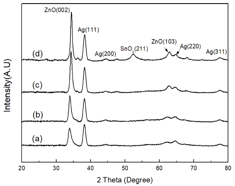
Figure 2 shows the XRD patterns observed from the ZAS tri-layer films as a function of electron irradiation energy. All of the XRD plots exhibited diffraction peaks of the Ag and ZnO planes regardless of the electron irradiation energy, while the characteristic diffraction peak for crystalline SnO2 did not appear for the low electron energy condition (≤ 600 eV). The films electron irradiated at 900 eV exhibited the diffraction peaks of SnO2 (211), ZnO (002), (103) and Ag (111), (200), respectively. Recently R. L. Orimi et al. [7] reported on the growth mode of polycrystalline SnO2 thin films deposited on glass substrate at 450 ◦C by chemical spray pyrolysis technique. However, it is supposed that the crystal growth of SnO2 film by electron irradiation commenced at 900 eV.
Table 1 shows the grain size (D) of the ZnO (002) and Ag (111) planes, considered by the Scherrer formula for each film:
where D is the grain size, λ is the X-ray radiation wavelength, B is the full-width at half-maximum (FWHM) of the diffraction peak, and θ is the Bragg angle of the diffraction peak [8]. Table 2 shows that the crystallite size in the ZnO and Ag interlayers increased with electron irradiation energy.
Figure 3 shows the AFM images of the as-deposited and the electron beam-irradiated ZAS films. While the asdeposited films showed an RMS roughness of 0.75 nm, the films electron-irradiated at 900 eV showed the lowest RMS roughness of 0.51 nm.
Figure 4 shows the optical transmittance of the ZAS films in the visible wavelength region. The as-deposited films showed an average visible transmittance of 80.8%, while the films electron-irradiated at 900 eV showed an increased average visible transmittance of 83.6%.
H. N. Cui [9] reported that surface scattering can cause a reduction in the optical transmittance of TCO thin films, with the optical scattering being caused either by surface microroughness, or by scattering at the film grain boundaries. From the XRD and AFM observation, the increased visible transmittance of the ZAS film is attributed to a flatter surface and larger grain size, resulting from the post-deposition electron irradiation.
Table 2 shows the figure of merit (FOM) as a function of electron irradiation energy. The FOM is an important index for evaluating the opto-electrical performance of TCO films. The FOM is defined as
where T is the average visible transmittance and Rsh is the sheet resistance [10]. The FOM reached a maximum of 3.86 × 10⁻² Ω−1 for the electron-irradiated films at 900 eV, higher than that of the as-deposited films, which was 1.06 × 10⁻² Ω−1. The electron beam irradiation enhances the temperature of ZAS film through energy transfer from the electron beam to the film. This may increase grain size and decrease the sheet resistance (increase the carrier density) of the film [11].
Figure 5 shows a plot of (αhν)2 of the ZAS films as a function of the photon energy. The optical absorption coefficient (α) can be calculated from the following Eq. (3) [12]:
where t is the film thickness, and T is the visible transmittance. The Tauc formula of Eq. (4) gives the relationship between the optical absorption coefficient (α) and optical band gap (Eg) [13]:
where hν is the energy of the incident photon, and A is the absorption edge width parameter. Figure 4 shows that as the electron energy increases to 600 eV, the optical band gap increases proportionally from 4.12 (as deposition) to 4.23 eV (at 600 eV). Table 3 shows the carrier density and optical band gap of the ZAS films as a function of electron irradiation energy. From the observed electrical properties and optical band gap, it can be concluded that the optical band gap shift is related to the carrier density of the films [14]. The band gap increased from 4.12 to 4.23 eV, with the carrier density increasing from 7.1 to 8.6 × 1021 cm−3. However, the film that was electron irradiated at 900 eV showed a decreased band gap energy of 4.16 eV, due to the decrease in carrier density of 8.2 × 1021 cm−3.
4. CONCLUSIONS
We deposited conductive and transparent ZnO 50 nm/Ag 10 nm/SnO2 50 nm tri-layer films onto glass substrates using RF and DC magnetron sputtering, and then exposed them to electron irradiation to investigate the effects of electron irradiation on the optical and electrical properties of the films.
In the XRD pattern and AFM images, the crystallite size was observed to increase with electron irradiation energy, and the films electron-irradiated at 900 eV showed the lowest RMS roughness of 1.30 nm. Due to the flat surface and enhanced crystallinity, the ZAS films electron-irradiated at 900 eV showed a maximum FOM of 3.86 × 10⁻² Ω−1, which was higher than that of the as-deposited films (1.06 × 10⁻² Ω−1).
Thus, we conclude that the electron beam irradiation effectively improves the optical and electrical performances of ZAS thin films.