


1. INTRODUCTION
Electroplated nickel-phosphorus (Ni-P) deposits are utilized in various industries such as automobile components, machinery, aerospace and electronics, because of their good physical, chemical and mechanical properties [1-7].
Usually, the electroless and electrodeposited Ni-P films are classified into three groups according to P content: high (9 wt% above), medium (5~8 wt%) or low (1~5 wt%) P deposits. Previous studies have revealed that the high P deposits have a fully amorphous-nanocrystalline structure [5,6,8], whereas the low and medium P deposits can be either crystalline or microcrystalline, with either amorphousnanocrystalline or mixtures of crystalline and amorphous-like structures [9,10].
In terms of properties like hardness and corrosion resistance, the microhardness of the electroless Ni-P deposit was increased by decreasing P content [5,6]. The Ni-P deposition has a higher dissolution rate than a conventional Ni deposit. The Ni-P deposit tends to be more uniformly corroded than the conventional Ni deposits because of its nanocrystalline structure which suffers excessive intergranular corrosion in acid atmosphere [11,12].
These kinds of mechanical and chemical properties of the Ni-P deposits can be controlled by the plating condition such as the temperature of the bath, pH and the type of additives. Lead acetate is known as a stabilizer in the electroless or electrodeposited Ni-P process. Since the toxic characteristics of the lead have limited the use of this stabilizer, some investigators have chosen other additives such as thiourea [13,14].
It is known that the thiourea enhances the deposition rate by lowering the activation energy of the deposition of the Ni ion [15]. In case of too much thiourea is adsorbed on the substrate, it can inhibit the deposition reaction by poisoning the catalytic activity of the accidentally formed NiP or metal hydroxide nuclei because of the effect of the thiourea on the surface coverage of the substrate [16].
Since the electroless Ni-P process is performed at about 90 ℃ and needs more time and energy, the electroplate process is preferred for Ni-P deposit in the field [21]. Although the effect of thiourea on electroless Ni-P deposits have been carried out, little information is available for the effect of thiourea on electroplated Ni-P deposits, especially about mechanical and chemical properties of the Ni-P deposit. Hence, the objective of this study is to investigate the effect of the thiourea on the mechanical and corrosion behavior of the electroplated Ni-P deposits in metallurgical point of view.
2. EXPERIMENTAL METHODS
2.1 Sample preparation
Ni-P deposits were prepared by conventional electrodeposition method with a modified sulfate bath. Table 1 is the bath of the Ni-P electrodeposition. The Ni-P bath solution is composed of a nickel sulfamate solution, phosphorous acid and boric acid, respectively. Various amounts of thiourea were added to the bath solution over the range of 0.01~0.1 g/L to observe the variation of the properties of the electroplated Ni-P deposits.
The titanium electrode and 304 stainless steel plate as a substrate were used. The substrate was electrolytic polished in 0.2N sulfuric acid (H2SO4) to remove debris and prepare a fine surface roughness prior to the electroforming of the NiP deposit. The Ni-P electrodeposition was conducted at 50 ℃ and 0.02 A/cm2 in the modified sulfate bath for an hour to have a similar thickness.
2.2 Microstructure, phase analysis and mechanical tests
Surface morphologies and cross sections were observed by atomic force microscopy (Pafm nx II, Em4sys, Korea) and scanning electron microscopy (CX-200TA, Coxem, Korea), respectively. The phase analysis was carried out by X-ray diffractometry (Ultima IV, Rigaku, Japan) at a diffraction angle from 30 o to 100 o, step rate of 0.02 o/sec and Cu·Kα line at room temperature. Chemical analysis was performed by energy dispersive spectroscopy (Noran, Thermo, USA). The mechanical properties of the Ni-P deposits prepared with and without thiourea was determined by dynamic nanoindentation method (Ti750, Hysitron, USA) for the specimens with similar thickness.
3. RESULTS AND DISCUSSION
3.1 Chemical analysis
Figure 1 and Table 2 are the composition variation of the Ni-P deposits with thiourea in the bath. As shown in Fig 1 and Table 2, the amount of Ni and P in the Ni-P deposits were 87.98, 96.74, 97.47, 98.91, 98.90 and 98.41 wt% and 12.12, 3.36, 2.53, 1.19, 1.10 and 1.59 wt%, respectively, as the thiourea content changed from 0.01 to 0.1 g/L. The P content in the Ni-P deposits decreased increasing the thiourea content in the bath solution whereas the Ni content increased the present data accords with the results reported by Lin et al. [14].
3.2 Phase identification
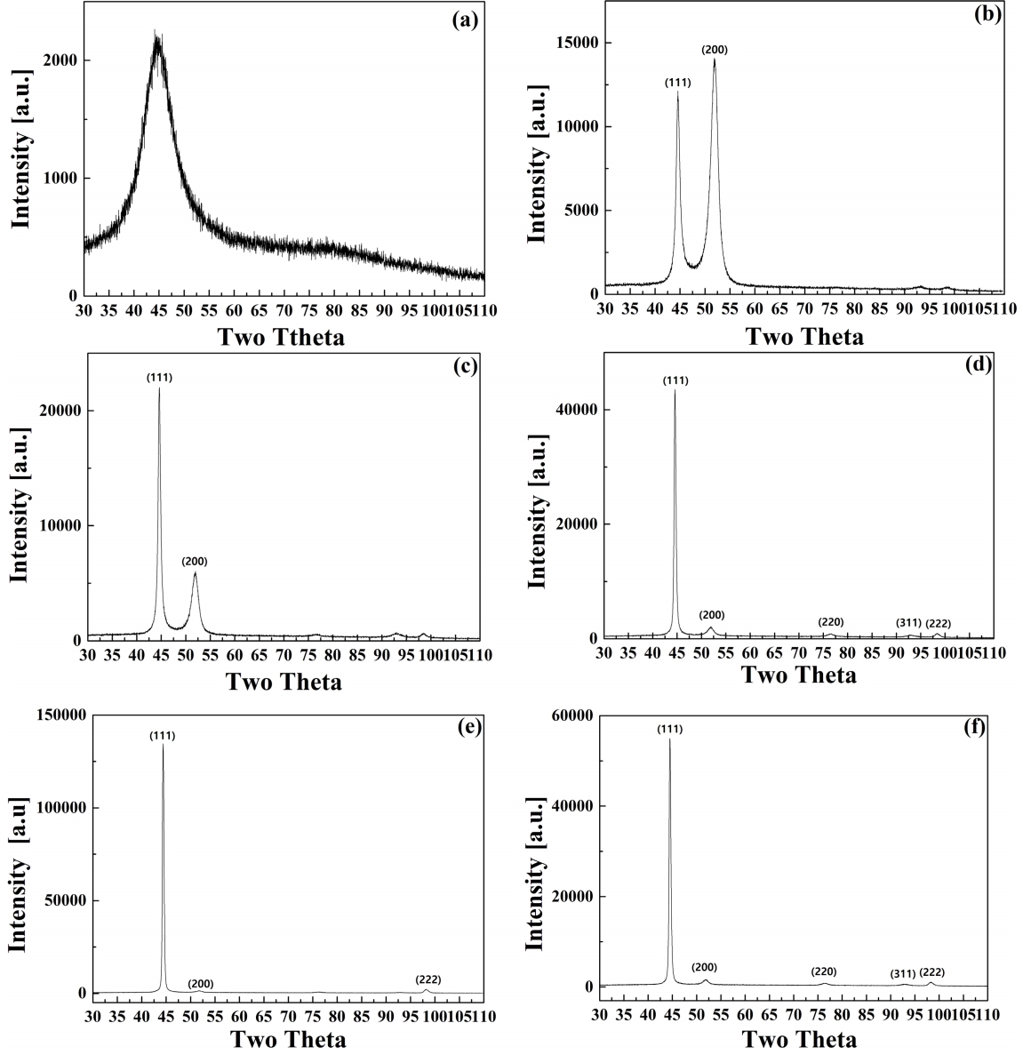
Figure 2 is the XRD spectra of the Ni-P deposits with thiourea. Figure 2-(a) is the spectra of the electrodeposited Ni-P layer without any additives. Figure 2-(b), (c), (d), (e) and (f) are the spectra of the electrodeposited Ni-P layers with thiourea in amounts of 0.01, 0.03, 0.05, 0.07 and 0.1 g/L, in order. As shown in Fig 2, the XRD spectra of the Ni-P deposit without thiourea has a broad peak in the range of 35~55o, which indicates an amorphous-nanostructure [6,9]. However, the XRD peaks for the deposits with thiourea show the crystalline structure with preferred orientations like splitting into planes of (111), (200), which indicates the crystalline Ni structure with face centered cubic structure (FCC) [10,20]. Considering these XRD peaks, the Ni-P deposits with thiourea are mainly composed of a Ni based structure. For the 0.01 g/L thiourea the intensity of (200) peak was higher than that of the (111) peak. As the amount of thiourea increased in the bath, the (111) peak of the Ni-P deposits increased and (200) peak decreased which dissipates entirely. It supports that the thiourea intensifies the (111) peak and crystallinity of the deposits. Since the amorphousnanostructure is formed for the Ni-P deposit with more than 7 wt% of P [15,17], the crystallinity of the Ni-P with thiourea is due to the low content of P of the Ni-P deposits [14].
3.3 Surface morphologies microstructure and mechanical properties
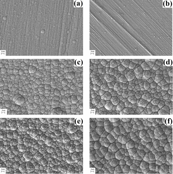
Figure 3 is the surface images of the electrodeposited NiP deposits with thiourea. As shown in Fig 3, the surface morphology of the Ni-P deposits without the additive and with 0.01 g/L thiourea has almost no nodules and relatively smooth and clean surfaces [18]. However, the surface morphologies of the Ni-P deposits with 0.03, 0.05, 0.07 and 0.1 g/L thiourea had more cauliflower-like nodules and subnodules on the surface of the deposits [19]. The surface roughness (RRMS) of the Ni-P deposits determined by atomic force microscopy increased from 6 to 54 nm with thiourea.
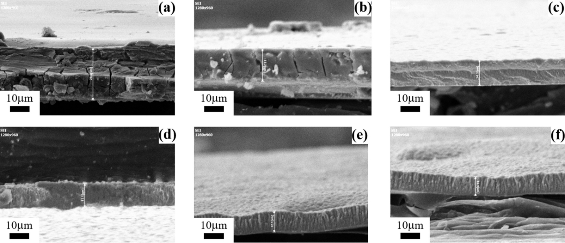
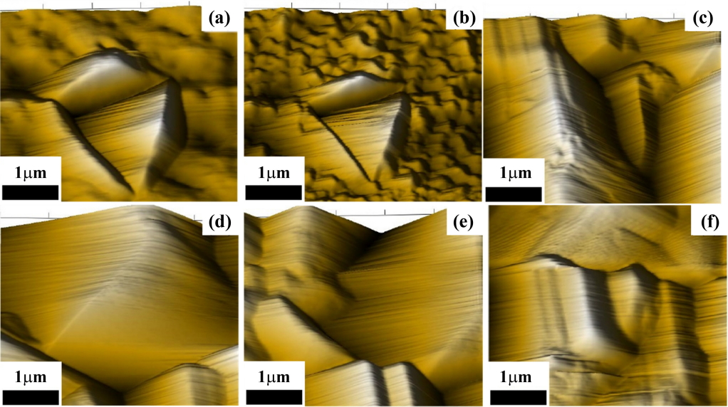
Figure 4 is the cross-sectional view of the Ni-P deposits with thiourea. As shown in Fig 4, the thickness of the Ni-P deposits with thiourea were 29.6, 18.2, 14.3, 13.5, 12.1 and 10.9 μm, respectively, which increasing the content of indicates that the thickness of the Ni-P deposits decreases with increasing the content of thiourea in the bath solution for the same plating time of one hour. Accordingly, the variation in the surface morphology and the reduction in thickness of the Ni-P deposits with thiourea can be attributed to the effect of thiourea on the grain growth of the nodules. The thiourea adsorbed on the surface of the substrate tends to retard the reduction of the Ni and P ions for the nucleation step. Figure 5 is the surface morphologies of the Ni-P deposits. As shown in Fig 4 and Fig 5, the size of the columnar grains tends to increase with increasing the content of thiourea.
Table 3 shows the surface roughness and mechanical properties of the Ni-P deposits with thiourea. As shown in Table 3, the surface roughness of the deposits increased from 6 to 54 nm with the addition of 0.1 ppm of thiourea. It implies that the average grain size of the columnar deposits increased with thiourea. The elastic modulus, hardness and stiffness of the Ni-P deposits increased by addition of 0.1 ppm of thiourea, from 77 to 156 GPa, 6.6 to 8.9 GPa and 109.6 to 186.6 μN/nm, respectively. Since the (111) plane of the deposits preferentially grew in Fig 2, the preferential growth in crystallinity is one of attributions on the nano-hardening of the Ni-P deposits with thiourea. Besides, the increase in stiffness and elastic modulus related to the decrease in P contents. According to the non-equilibrium Ni-P binary phase diagram, the Ni-P deposits with a low, medium and high P content consist of β(crystalline), β+γ(crystalline + amorphous) and γ(amorphous) phases. Since the β phase has greater hardness than the γ phase, the nano-hardness of the Ni-P deposits increased as the P content decreased [6].
4. CONCLUSIONS
1. The P content of the Ni-P deposits decreased with increasing thiourea content in the bath, whereas, the Ni content of the deposits increased with thiourea.
2. The thiourea intensified the (111) peak and crystallinity of the electrodeposited Ni-P deposits.
3. The surface morphologies of deposits without additive and with 0.01 g/L of thiourea had almost no nodules and were relatively smooth and clean. Those of the Ni-P deposits with 0.03, 0.05, 0.07 and 0.1 g/L thiourea had more cauliflower-like nodules and sub-nodules on the surface. The surface roughness of the Ni-P deposits determined by atomic force microscopy increased from 6 to 54 nm with the addition of 0.1 ppm of thiourea.
4. The elastic modulus, hardness and stiffness of the Ni-P deposits with thiourea increased from 77 to 156 GPa, 6.6 to 8.9 GPa and 109.6 to 186.6 μN/nm, respectively. The hardening of the Ni-P deposits with thiourea is related to the preferential growth of crystallinity and P content. Increased stiffness and elastic modulus resulted from a decrease in P content which led to the β phase instead of γ phase.