Tin Microcrystals Synthesized by Thermal Chemical Vapor Deposition in a Hydrogen-Reducing Atmosphere
Article information
Abstract
We demonstrate a synthetic route to high-quality Sn microcrystals using thermal chemical vapor deposition (CVD) in a hydrogen-reducing atmosphere. During thermal CVD with SnO2 powder, a mixture of Ar and H2 (4%) gases was used as a carrier gas to maintain a hydrogen reduction environment. Hydrogen maintained a reduction environment throughout the thermal CVD process. Samples were prepared at temperatures of 800, 900, and 1000 °C. The structural properties of the Sn microcrystals were determined using synchrotron X-ray diffraction (XRD), transmission electron microscopy, and micro-Raman spectroscopy. In particular, the atomic position order in both the out-of-plane and in-plane directions was determined through high-resolution XRD measurement in a four-circle geometry. We found that at temperatures greater than 800 °C the supersaturation of Sn and O vapors induces the formation of microcrystals by self-assembly process without additional metallic seeds. As determined by the energy dispersive X-ray analysis, oxygen atoms and/or vapor were simultaneously reduced by hydrogen gas, resulting in the formation of Sn crystals rather than Sn oxide crystals. We also found that the Sn microcrystals were mostly strain-free single-crystalline and of high quality with extremely low mosaicity. The order of the atomic positions in both the out-of-plane and in-plane directions was comparable to that of single-crystalline sapphire.
1. INTRODUCTION
Recent advances in the assembly of metallic crystals have enabled the exploration of next-generation electrochemical and photovoltaic devices such as batteries and solar cells [1,2]. Among various additives, Sn nanocrystals are effective for carbon-based or Si-based anode materials to promote the lithiation reaction and decrease charge transfer resistance in lithium-ion batteries [4-8]. They have also recently been investigated for use in highly conductive inks for inkjet printing, to fabricate flexible electronic devices [9]. Superconducting Sn nanocrystals are also employed to investigate the nature of zero-dimensional superconductors and quantum size effects [10,11]. To synthesize monodisperse Sn crystals with tunable size and shape, chemical synthetic routes using reducing agents have typically been used, and their properties and device performance have been reported [12-16].
As an alternative to solution-based techniques, thermal chemical vapor deposition (CVD) using SnO2 powder can be used to obtain high-quality one-dimensional nanostructures such as nanowires and nanorods. In the vapor–liquid–solid (VLS) mechanism, metallic seeds initiate the growth of SnO2 nanowires [17,18]. Moreover, crystals can be obtained when the deposition conditions are optimized, for example, at high process temperatures (greater than 800 °C). The resulting Sn crystals are high quality with a remarkably low defect density and mosaicity, and can be utilized as a platform to study the physical properties of Sn, including oxidation kinetics and reaction behaviors with other metals, such as Pt and Li [19,20]. In this study, Sn single crystals were synthesized via thermal CVD without seeds in a hydrogen atmosphere. Hydrogen reduces oxygen atoms or vapor, resulting in the formation of Sn crystals rather than Sn oxides. The microstructures of the Sn crystals were characterized using transmission electron microscopy (TEM), micro-Raman spectroscopy, and synchrotron X-ray diffraction (XRD). In particular, the atomic position order in both the out-of-plane and in-plane directions was determined using high-resolution XRD measurement in a four-circle geometry.
2. EXPERIMENTS
Sn microcrystals were synthesized using thermal CVD in a hydrogen-reducing atmosphere. The details of the thermal CVD method have been described previously [17]. Before the thermal CVD, sapphire(001) substrates were cleaned using a standard process and placed on top of an alumina boat containing SnO2 powder (High Purity Chemicals Co., #SNO03PB) as a source material. The thermal CVD system was evacuated and heated to a desired temperature at a ramping rate of 10 °C/min. Samples were prepared at temperatures of 800, 900, and 1000 °C. When the system reached the process temperature, a mixture of Ar and H2 (4%) gases was introduced as the carrier gas at a flow rate of 40 sccm using a mass flow controller. The hydrogen maintained a reduction environment throughout the thermal CVD process [17,21]. A working pressure of 5 Torr was maintained for 2 h, and then the thermal CVD system was cooled to 25 °C.
The surface morphology of the as-prepared samples was examined using scanning electron microscopy (SEM, Hitachi S-4700). The atomic structure of the microcrystals was determined using TEM (Tecnai F20, operated at 200 keV). A microcrystal sample was sectioned using a focused ion beam technique (FEI Quanta 3D FEG) with a Ga ion-beam source; it was then mounted on a Cu grid for TEM measurement. To determine the chemical composition of the microcrystals, energy-dispersive X-ray (EDX) analysis was performed during TEM measurement. The structural properties of the Sn crystals were characterized using high-resolution synchrotron XRD measurements at the 5D beamline of the Pohang Light Source-II. Typical θ–2θ XRD profiles and θ rocking curves were measured to determine the atomic planes along the surface normal direction and the mosaicity of the crystals, respectively. In particular, the off-specular Sn(200) Bragg peaks were examined using a four-circle geometry, which allowed us to determine the single-crystal characteristics of the microcrystals. ϕ scans of the Sn(200) and sapphire(113) Bragg peaks were performed to evaluate the atomic position order in the in-plane direction. Finally, the micro-Raman spectrum of an isolated Sn crystal was obtained at 25 °C. An Ar laser with a wavelength of 514.5 nm was used as the excitation source. The laser focus was approximately 8 μm in diameter and illuminated a single microcrystal.
3. RESULTS AND DISCUSSION
First, we discuss the morphology of the as-grown samples. Figure 1 shows a series of top-view SEM images of as-grown samples prepared at 800 °C [(a) and (b)] and 1000 °C [(c) and (d)]. The images show that the surface morphology of the samples consists of distributed individual crystals. Most of the crystals appear round in the top-view images and have different diameters, which depend significantly on the growth temperature. In the sample grown at 800 °C, the diameters of the crystals vary between 0.55 and 1.2 μm, whereas it ranges from 7 to 21 μm in the sample prepared at 1000 °C. Note that samples prepared at 900 °C show similar morphologies with different microcrystal diameters (data not shown). Microcrystal formation with no additional metallic seeds can be explained by a self-assembly process. Thermal CVD typically proceeds by self-assembly to form nanostructures such as nanowires and nanocrystals. The reaction (supersaturation) of vapors typically follows either the VLS mechanism with metal seeds or the vapor–solid (VS) mechanism [22]. The former produces nanowires, and the latter forms mostly crystals. In this study, SnO2 powder was dissociated into Sn and O vapors, which were supersaturated during the thermal CVD. Self-assembled seeds, i.e., possible Sn clusters, were simultaneously nucleated on the surfaces and then at temperatures greater than 800 °C grew to form microcrystals rather than nanowires. It might be speculated that hydrogen reduction continues to limit the VLS process, which would produce nanowires. Indeed, the VS mechanism depends significantly on the process temperature and pressure, as demonstrated by the significant increase in the diameters of the crystals from nanometer-scale to tens of microns as the temperature increased from 800 to 1000 °C in this study. The mechanism is also quite sensitive to pressure, and 1~5 Torr is optimal for obtaining crystals. Although the top-view SEM images revealed round shapes, the bird’s-eye view SEM image in Fig 1(d) indicates that the microcrystals are hemispherical rather than completely spherical. This can be explained by a Winterbottom analysis of a single crystal [23,24]. The height of a hemisphere in the vertical direction is estimated to be approximately 3/4 of the diameter.

Top-view SEM images of samples prepared at (a),(b) 800 °C and (c),(d) 1000 °C. Hemispherical microcrystals are observed.
The SEM results confirmed the formation of microcrystals by thermal CVD in a hydrogen atmosphere. We postulate that the microcrystals are Sn rather than Sn oxide because hydrogen reduction eliminated the oxygen atoms at temperatures greater than 800 °C. To determine the atomic structure and chemical composition of the microcrystals, we performed TEM measurement and EDX analysis. Figure 2(a) shows a cross-sectional TEM image, which illustrates the hemispherical shape of a crystal. The bright area corresponds to the sapphire(001) substrate. A Pt/C capping layer surrounds the microcrystal. Figure 2(b) shows the EDX profile measured in the center of the hemisphere to avoid the contribution of the sapphire substrate. The peak at E = 3.45 keV corresponds to the characteristic L emission of Sn atoms, whereas the characteristic K emission from oxygen atoms (E = 0.52 keV) is negligible. Note that characteristic carbon, nitrogen, and copper emissions are detected at E = 0.28, 0.39, and 8.05 keV, respectively. Most of these atoms are located in the Cu TEM grid.
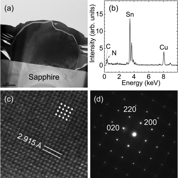
(a) Cross-sectional TEM image, (b) EDX profile, (c) high-resolution TEM image, and (d) TED pattern of a single Sn crystal. Yellow dots in (b) represent the lattice position of the tetragonal phase of Sn.
EDX analysis reveals that the microcrystals are Sn crystals rather than Sn oxide crystals, which was also manifested in the high-resolution TEM image in Fig 2(c). The TEM image clearly shows the atomic arrangement of the microcrystals. A square periodic unit with four-fold symmetry is indicated in the figure. The layer spacing is estimated to be 2.915 Å in both the vertical and horizontal directions, which corresponds to the lattice spacing of the (200) planes of Sn crystals (JCPDS #89-4898). In addition, a selected area transmission electron diffraction (TED) pattern is shown in Fig 2(d); the primary diffraction spots are indexed as the (020), (220), and (200) planes. This strongly confirms that Sn crystals were formed by thermal CVD in a hydrogen atmosphere. No halfinteger index spots or forbidden index spots can be detected, indicating that defects such as dislocations and stacking faults, are negligible. It is noted that the Sn crystals would be liquid at the growth temperatures, but they were transformed into a solid when the temperature was decreased to RT after growth.
Studying the structural properties of the as-prepared samples using high-resolution XRD measurements clarifies the formation of the Sn microcrystals. Figure 3(a) shows the XRD profile of the sample grown at 1000 °C. Two peaks are clearly detected and are indexed as the Sn(101) Bragg peak at Q = 2.25 Å-1 and sapphire(006) Bragg peak at Q = 2.9 Å-1. Note that Q is the X-ray momentum transfer and is equal to 2π/d, where d is the lattice spacing. The Sn(101) Bragg peak was fitted to a simple Gaussian profile. The full width at half maximum (FWHM) was 0.00234 Å-1, which corresponds to a domain size of approximately 270 nm [25]. In addition, the lattice spacing of the (101) planes calculated using the peak position was 2.7925 Å, which is quite similar to the bulk value of 2.7931 Å. This means that the microcrystals are mostly strain-free in the surface normal direction, although they were prepared on a sapphire(001) substrate. A possible origin of the strain-free state is related to the growth mechanism. Sn microcrystals are in liquid form at the growth temperatures and are transformed into solids during the cooling process. This is in contrast to the typical deposition on substrates, where misfit strain between the thin films and the substrate is inherent from the initial stage of growth. In addition, their thickness of several micrometers also allows full relaxation of the lattice mismatch between the Sn microcrystals and sapphire(001) substrate.

(a) XRD θ–2θ scan profile of sample prepared at 1000 °C. (b) θ rocking curve of the Sn(101) and sapphire(006) Bragg peaks.
The mosaicity of the Sn microcrystal was evaluated from the θ rocking curve shown in Fig 3(b). This rocking curve was measured at the Sn(101) Bragg peak. The rocking curve of the sapphire(006) Bragg peak is also displayed for comparison. The peaks are quite sharp; the FWHM of the sapphire(001) peak is 0.0037°, and that of the Sn(101) peak is 0.0098°, indicating that the Sn microcrystals are of high quality with extremely low mosaicity [25].
To determine the single-crystalline nature of the Sn microcrystals, off-specular Sn(200) Bragg peaks in a four-circle geometry were examined. Figures 4(a) and (b) show the XRD profiles of the off-specular Sn(200) Bragg peak in the H and L directions, respectively, where H and L are the reciprocal space coordinates. The scan geometry in reciprocal space is shown schematically in the inset of Fig 4(a). The chi angle (interplanar angle) between the (101) and (200) Bragg peaks is approximately 61.4°. The FWHM values of the H and L scans are 0.00126 and 0.00225 Å-1, respectively. They correspond to an in-plane domain size of 500 nm and an out-of-plane domain size of 280 nm [25]. The out-of-plane domain size is quite similar to that estimated from the out-of-plane (101) Bragg peak shown in Fig 3(a). The d spacing of the (200) planes was found to be 2.9169 Å, which is also similar to the bulk value of 2.9155 Å. This also supports the mostly strain-free state of the Sn microcrystals.

(a) H scan, (b) L scan, and (c) ϕ scan of off-specular Sn(200) peak. Schematic in (a) illustrates the reciprocal space coordinates of the Sn(101) and Sn(200) peaks. The ϕ scan of the off-specular sapphire(113) peak is also displayed in (c) for comparison. FWHM of the ϕ scan represents the atomic position order of the crystals in the in-plane direction.
The atomic position order in the in-plane direction was evaluated by a ϕ scan of the Sn(200) Bragg peak, as shown in Fig 4(c). A ϕ scan of the sapphire(113) peak is also shown for comparison. The FWHM of the sapphire(113) peak is approximately 0.005°, whereas that of the Sn(200) peak is estimated to be 0.0083°. This indicates that the structure of the Sn microcrystals is entirely coherent and of high quality [25,26]. The off-specular XRD measurement confirmed the single-crystalline nature of the Sn microcrystals.
Figure 5 shows a micro-Raman spectrum of a single Sn microcrystal prepared at 1000 °C, which indicates the optical phonon modes of the Sn microcrystals. Theory predicts two vibrational frequencies of the optical Γ-point phonons: the Γ3 phonon mode in the longitudinal direction at 45 cm-1 and the Γ5 photon mode in the transverse direction at 130 cm-1 [27,28]. Raman spectroscopy shows a dominant peak at 127.15 cm-1, which can be indexed as the Γ5 phonon mode, because it matches the theoretical value well. The strong Raman spectrum supports the high quality of the crystal. Note that the Γ3 phonon mode peak was not detected because of the noise level, which posed a detection limit of 100 cm-1 in the Raman spectroscopy used in this study. It is noteworthy that the intensity of the Raman spectra is highly proportional to the size of the crystals (data not shown). We expect that the Raman scattering results can serve as a platform to explore the oxidation behavior of Sn single crystals, where the phase should be transformed from Sn to SnO2 through intermediate states such as SnO, Sn2O3, and Sn3O4 [29,30].
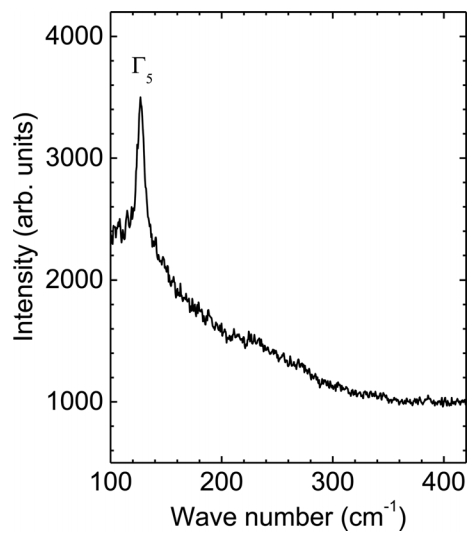
Micro-Raman spectroscopy profile of a single Sn microcrystal prepared at 1000 °C. Peak detected at 127.15 cm-1 corresponds to the Γ5 phonon mode of Sn in the transverse direction.
4. CONCLUSIONS
In summary, we examined the use of thermal CVD and SnO2 powder in a hydrogen-reducing atmosphere to synthesize Sn microcrystals. We found that at temperatures greater than 800 °C the hydrogen reduction environment during thermal CVD was quite effective for forming Sn microcrystals. The Sn crystals were single-crystalline, and the order of the atomic positions in both the out-of-plane and in-plane directions was comparable to that of single-crystalline sapphire. Because high-quality Sn crystals with low defect density can be used as a host material to investigate the melting or oxidation kinetics of Sn, we plan to conduct an insitu XRD experiment during melting or oxidation.