Nucleation and Growth-Controlled Morphology Evolution of Cu Nanostructures During High-Pressure Thermal Evaporation
Article information
Abstract
The formation of porous material structures has been widely investigated for the development of high-performance energy materials, catalysts, and chemical sensing devices. Various nanoporous structure fabrication methods are based on wet-chemical processes, which require precise control of the process parameters. Physical vapor deposition such as thermal evaporation utilizes high vacuum so that the deposition process is relatively simple, free of contamination, and easily reproduced. However, because of the long mean-free-path of the evaporated atoms in high vacuum, heterogeneous nucleation and the growth of adatoms occurs on the substrate surface, which results in the formation of dense and compact thin films. But by changing the working pressure, various morphologies of porous nanostructures can be obtained. As applied to copper, with increasing pressure the thin film evolves from a dense structure to a coral-like nanoporous structure through a porous columnar structure. All of the porous structures consist of nanoparticle aggregates, where copper nanoparticles are connected to each other, and many nano-gaps are found inside the aggregates. A surface plasmonic effect is expected. The porous copper nanostructured films demonstrated high surface-enhanced Raman spectroscopy activity.
1. Introduction
Materials frequently exhibit new features when they are synthesized in nano scale. Nanostructured materials in the forms of nanospheres [1-3], nanocubes [4-6], nanorods [7-9], and nanodendrites [10-13] have attracted considerable interest because of their unique characteristics. Processes producing those nanostructured materials generally require complex routes. For example, electrochemical synthesis produces various nanostructure morphologies by controlling voltage, current, time, and pH of the electrolyte, and so on.
Well-defined core-shell or hollow-nanospheres also require multiple steps. Stacking of nanowires should be accompanied by additional separation and alignment processes [14-18].
Given their complexity, there is considerable value in developing simple ways to synthesize nanostructured materials. Herein, we introduce a vacuum-mediated, clean, simple method to fabricate nanostructures of certain metals. By filling the evaporation chamber with an inert gas and just controlling the pressure, various morphologies of metal films can be achieved, from dense and compact ones to nanoporous ones. L. Harris et al. first demonstrated this technique in the 1940s [19] and succeeded in making nanostructured gold.
However, there have been no systematic studies that clarify the relationship between morphology and control parameters like pressure. In this research, copper was chosen for the systematic study because of its melting point similar to gold and various promising catalytic properties. The nanostructure of copper evolves from a dense thin film to a highly porous structure through a columnar structure as the pressure increases. In addition, the porous columnar structure and the nanoparticle aggregates obtained through this process include nano-gaps that can induce surface plasmonic effects. The application of the nanostructured copper for surface-enhanced Raman spectroscopy (SERS) is further discussed.
2. Experimental
Materials: 5N high purity copper pellets of 3 mm diameter and 3 mm thickness (TASCO, USA) were used as the thermal evaporation source. Rhodamine 6G (BioReagent) from Sigma Aldrich was used as the probe molecules.
Fabrication of copper nanostructure: A copper pellet of 0.228 g is placed on a tungsten boat and a Si substrate is mounted on the water-cooled copper block inside the designed thermal evaporation vacuum chamber, as shown in Fig 1. The distance between the evaporation source and the substrate is 7.5 cm. After evacuating the chamber, the desired pressure is set, with 5 sccm Ar flow prior to deposition. The thermal evaporation is carried out at 350W. Water-cooling maintains the substrate temperature at around 100 °C during the evaporation, which prevents agglomeration of the nanoparticles arriving at the substrate.
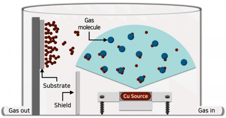
Schematic description of the formation of porous nanostructures using high-pressure thermal evaporation.
Characterization: Field emission scanning electron microscopy (FE-SEM) analysis was performed using JSM-7610F PLUS (JEOL, Japan) at an accelerating voltage of 15 kV.
Transmission electron microscope (TEM) images were acquired using a Tecnai F20 (FEI Company, USA). X-ray diffraction (XRD) data was collected from Empyrean (Malvern Panalytical, UK). Reflectance was obtained using a Cary 5000 (Varian, USA) UV/Visible/NIR spectrophotometer with the base line from PTFE. The contact angles for a 10 μL volume of water dropped on the surface of the nanostructured copper were measured by a contact angle measurement system (Surface Electro Optics, Phoenix-I, South Korea) under static condition.
Evaluation of SERS activity: Rhodamine 6G (R6G) was used as a probe molecule in SERS experiments due to its well-established vibration features and Raman shifts. After dilution in de-ionized (DI) water, R6G solutions of 10-4 M to 10-9 M were prepared. To evaporate the water all samples were dried in an oven of 40 °C. The spectra were collected under ambient conditions using the 532 nm line of a diode pumped solid state (DPSS) laser with 120 μW irradiation of the sample surface. The data acquisition time and the number of accumulations were 5 s and 2, respectively.
3. Results and Discussion
3.1 Nanostructured copper formed by nucleation and growth control during evaporation
During the conventional thermal evaporation process under high vacuum, the evaporated atoms have a long mean free path. The size of adatoms arriving at the substrate are so small that they have high surface mobility. Due to the promoted surface diffusion the adatoms can easily move to defect sites like kinks, and heterogeneous nucleation and growth occur. If the working pressure increases, on the other hand, the evaporated atoms collide with the gas molecules with increasing frequency, causing homogenous nucleation and growth, producing large clusters of the source material before reaching the substrate. On the substrate, the surface mobility of the clusters is too low to diffuse, and therefore, they easily form nanoparticle aggregates.
This nucleation and growth-controlled process to fabricate nanoporous structures is described schematically in Fig 1. By applying this process to copper, various copper film morphologies were obtained at different working pressures, as shown in Fig 2. Dense thin films of copper were obtained under high vacuum, resembling the typical thermal evaporation process of metals. However, as the pressure was increased to 0.01 Torr, columnar grains began to form with surface cracks.
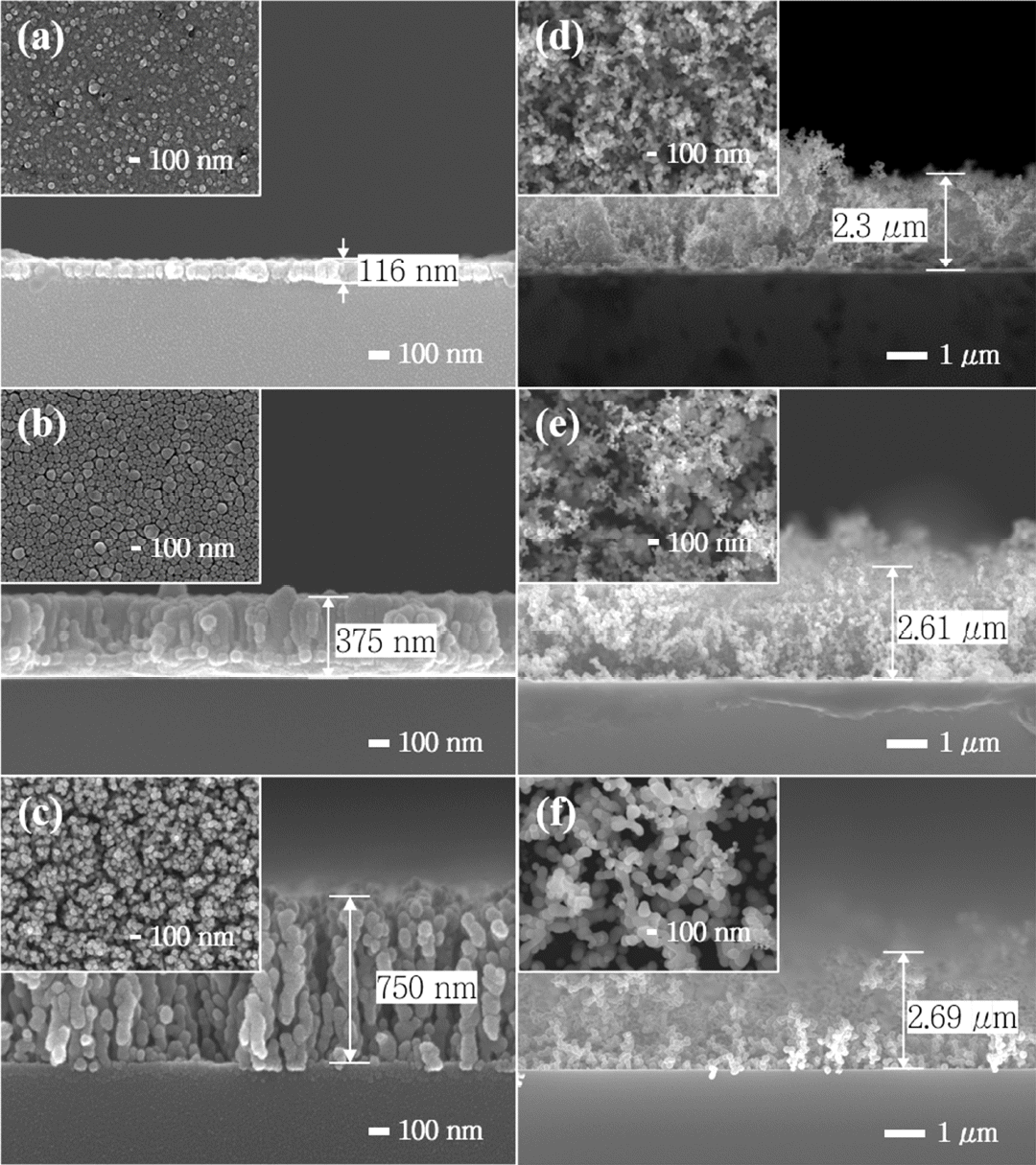
FE-SEM analysis of the evolution of the copper nanostructures with pressure: (a) < 10-6 Torr, (b) 0.01 Torr, (c) 0.1 Torr, (d) 1 Torr, (e) 2 Torr, (f) 4 Torr.
Interestingly, this columnar structure became more obvious as the pressure increased to 0.1 Torr, where the individual column had a high aspect ratio and pores were found between these columns. As the pressure increased further, the pattern of growth changed. At 1 Torr and above, highly porous structures were formed and the nanoporous films became much thicker than the columnar structured films grown at lower pressure. As shown in the SEM images, these coral-like nanostructures consist of nanoparticle aggregates, and much larger pores are observed. This is because the nanoclusters formed during the traverse to the substrate are physically adsorbed onto the previously grown nanostructures and do not move on the surface due to the low surface mobility, as mentioned earlier. As a result, some large pores extend to the bottom of the film so that the substrate surface is partially exposed.
Because the pores are so large, the BET method cannot be applied to measure porosity. Instead, the porosity can be estimated by the weight of the deposits, the dimensions determined from SEM images and the theoretical density of copper. The porosity increased from 14.14% (0.01 Torr) to 87.89% (1 Torr) as expected from the SEM analysis. Note that the individual nanoparticles are crystallographically bonded to each other, as verified by TEM analysis (Fig 3(a)) although physical adsorption weakens the adhesion of the nanoparticle aggregates to the substrate.
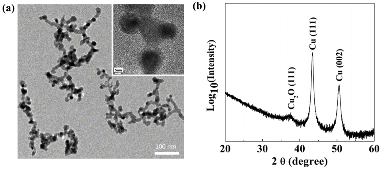
(a) TEM image of copper nanoparticle aggregates. Inset is the magnified view that shows copper nanoparticles bonded to each other. (b) XRD pattern of the nanoporous copper deposited at 1 Torr.
Because the whole structure consists of nanoparticles, the porous copper is slightly oxidized, as confirmed by XRD analysis in Fig 3(b). The diffraction peaks of the nanostructure were indexed to pure copper with lattice constant of a=3.61 Å, where the diffraction peaks at 2θ values of 43.4148° and 50.5632° are ascribed to the reflection of the (111) and (200) planes of the cubic copper (JCPDS No. 98-005-3756), respectively.
There is an additional peak that corresponds to Cu2O (111) viewed in log scale. The oxidized phase might exist at the bonded region, similar to nanoporous Sn [20]. This can be clearly established with more precise TEM analysis.
The different surface states were further examined by measuring the contact angles of water droplets, as summarized in Fig 4. As the morphologies evolve from a dense structure through porous columnar structure to nanoporous structure, the hydrophobicity becomes enhanced. There was no obvious tendency in the contact angle beyond 1 Torr, which might be due to the irregularly formed surface and the reduced surface coverage.

Contact angles of copper nanostructure deposited at different pressure: (a) < 10-6 Torr, (b) 0.01 Torr, (c) 0.1 Torr, (d) 1 Torr, (e) 2 Torr, (f) 4 Torr. Contact angles of both right and left side are averaged.
3.2 Changes in optical reflectance and SERS activity
Along with the evolution of the structures depending on the deposition pressure, the optical properties of the copper nanostructures changed dramatically, as shown in Fig 5(a). Thin films grown under high vacuum (< 10-6 Torr, not shown) and at 0.01 Torr showed high reflectance across the visible and NIR range, as is generally expected from the shining surface of metallic copper films. However, as the pressure was increased over 0.1 Torr, the resulting copper nanostructures absorbed visible and NIR spectra. In particular, copper nanostructures grown at 0.5 Torr and 1 Torr showed a reflectance of less than 5%, which makes these nanostructures black, as presented in the inset. The slight increase in reflectance of the nanostructure grown at 0.1 Torr is because the structure was in the middle of transition, from a compact dense film to a highly porous film. The high reflectance of the copper nanostructure formed at 4 Torr was caused by reflection from the uncovered area of the substrate.
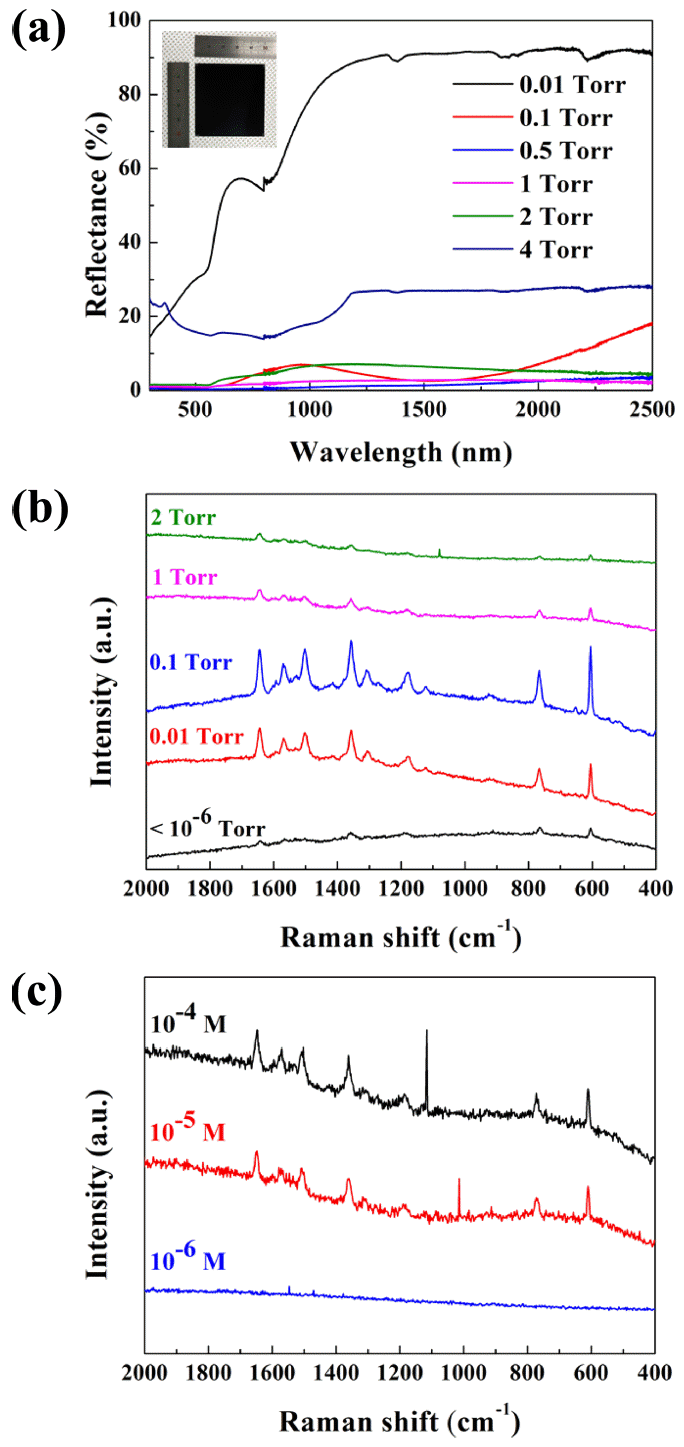
(a) UV/visible/NIR reflectance spectra of copper nanostructures deposited at different pressure. Inset is the copper nanostructure formed at 1 Torr that absorbs most of the visible light showing black color. (b) Raman spectra of rhodamine 6G (10-4 M) dropped on the copper nanostructures. (c) Raman spectra of rhodamine 6G with different concentration dropped on the copper nanostructure formed at 0.1 Torr.
The nanostructures with multiple nanogaps, as found in the SEM and TEM analyses, and the optical properties that absorbed most of the visible light led us to the possible application in SERS, where Raman scattering signals are enhanced by adapting various nanostructures on the metal surfaces. Due to the tremendous number of nano-gaps in the columnar nanostructure (Fig 2(c)) as well as the nanoparticle aggregates (Fig 2(d)-2(f)), these structures are expected to have greatly enhanced SERS activity, even though SERS activity is known to be enhanced only by nanostructured noble metals such as gold and silver.
To verify this hypothesis, we examined the SERS activity of the various nanostructures grown at different pressures. Compared to the compact thin film, the columnar porous structure grown at 0.1 Torr exhibited the highest SERS activity for the R6G molecules, of 10-4 M, as shown in Fig 5(b). This can be explained by the hydrophobicity and aspect ratio of the copper nanostructures. To achieve high SERS sensitivity, analytes should be located in or around the socalled “hot spots” which are normally formed in sub-10 nm gaps between neighboring plasmonic nanostructures. Hydrophobic nanostructures have advantages over hydrophilic ones, in that matter and probe molecules can be effectively accumulated on the SERS-active sites [21,22]. According to previous studies [23-25], as the aspect ratio increases, the light scattering inside the structure is enhanced because the number of probing molecules within the detection volume increases as well. These factors contribute to the stronger light-metal and light-molecule interaction, which then leads to higher SERS activity.
Note that the more highly nanoporous structures synthesized at 1 Torr and above, instead demonstrated much reduced SERS activity. This supports previous studies that surface roughness offering nanosized gaps for localized surface plasmonic resonance (LSPR) does not play a substantial role, but the shape of the nanostructures does [25-27].
The SERS sensitivity of the copper nanostructure fabricated at 0.1 Torr was also measured using various concentrations of R6G from 10-4 to 10-9 M. The SERS intensity was still observable at 10-5 M although SERS activity was almost lost below 10-6 M. Further research is being conducted to enhance SERS sensitivity.
4. Conclusions
High-pressure thermal evaporation has been employed to create copper nanostructures. As the pressure was increased, the thin film gradually evolved from a dense, compact structure through a porous columnar structure to a highly porous structure. This is due to the promotion of homogeneous nucleation and the layered growth of evaporated atoms by repeated collision with each other, due to the increased pressure and low surface mobility on the substrate surface. Microscopic analysis revealed that both the porous columnar structures and irregular nanoporous structures consisted of nanoparticle aggregates with nano-gaps. The plasmonic effect from these nano-gaps was observed, and the as-made copper nanostructures showed enhanced SERS activity for R6G molecules, which was not observed from a dense copper film. The measured sensitivity was down to a concentration of 10-5 M. Although the degree of enhancement is not as high as nanostructured gold or silver, it is meaningful that this approach involved a low-cost process using a simple evaporation method and copper for a chemical sensor. Furthermore, this high-pressure thermal evaporation method can provide a more cost-effective way to mass produce gold or silver SERS substrates or to fabricate highly sensitive Snbased gas sensors [28].
Acknowledgements
This work was supported by Kyonggi University's Graduate Research Assistantship 2019 and the National Research Foundation of Korea (NRF) grant funded by the Korea government (NRF-2019R1F1A1064146).