Effects of Blended Poly(3-hexylthiophene) and 6,13-bis(triisopropylsilylethynyl) pentacene Organic Semiconductors on the Photoresponse Characteristics of Thin-Film Transistors
Article information
Abstract
In this study, we demonstrate high-performance optical wavelength-selective organic thin-film transistors (TFTs) that incorporate heterogeneous organic semiconductor materials, poly(3-hexylthiophene) (P3HT) and 6,13-bis(triisopropylsilylethynyl) pentacene (TIPS-pentacene). The electrical characteristics of the fabricated transistors were analyzed in the dark to determine how the P3HT:TIPS-pentacene ratio of the semiconductor affected the performance of the transistor. Specifically, the P3HT:TIPS-pentacene weight ratio was varied (1:0, 1:0.25, 1:0.5, 1:0.75, 1:1, and 0:1) by blending 1 wt% P3HT dissolved in chloroform, and 1 wt% TIPS-pentacene dissolved in anisole. The UV-visible light absorbance characteristics of the films containing the P3HT, TIPS-pentacene, and P3HT:TIPS-pentacene blends were analyzed. Monochromatic light at wavelengths of 515 and 450 nm was used to clarify the influence of irradiation on the electrical characteristics of the TFTs. The results confirmed that the TFT containing P3HT:TIPS-pentacene at a blending ratio of 1:0.5 had the largest light-to-dark current ratio, i.e., approximately 33.8 and 23.5 when exposed to monochromatic light at wavelengths of 515 nm and 450 nm, respectively. The TFT with the P3HT:TIPS-pentacene blending ratio of 1:0.5 exhibited the highest photosensitivity values of 261.9 and 49.6 upon irradiation with light at wavelengths of 515 nm and 450 nm, respectively. The observed improvement in the performance of the heterogeneously blended organic transistors is discussed in relation to the morphological structure and charge transport path of the P3HT:TIPS-pentacene blended semiconductor films.
1. Introduction
Organic semiconductors have electrical and optical properties, which make these materials good candidates use in conventional semiconductor devices such as light-emitting diodes, photovoltaic cells, and thin-film transistors. An additional advantage is their absorption and emission properties in the visible wavelength range. Compared with silicon-based phototransistors, which are used extensively in conventional photoelectric sensors, organic phototransistors (OPTs) have an excellent light absorption coefficient and exhibit optical response characteristics that are determined by the light absorption properties of the organic semiconductor material, thereby obviating the need for color filters [1,2]. Accordingly, inorganic semiconductors are being replaced by organic semiconductors, which can reduce photon loss and simplify the light absorption process [3,4]. Compared with photodiodes, phototransistors are more efficient because of their higher sensitivity to light and lower sensitivity to noise interference, and the photocurrent can be modulated by varying the voltage applied to the gate (VG) and by irradiating with light [5,6]. OPTs have already found application in imaging sensors, optical communications, and biomedical sensors [7-9]. Numerous organic semiconductors have been proposed for the active layer of OPTs, but do not meet the requirements of the application. In efforts to improve their performance, further studies have focused on mixed and composite TFTs which combine the advantages of organic semiconductors and OPTs.
In this study, the electrical characteristics of TFTs based on poly(3-hexylthiophene) (P3HT):6,13-bis(triisopropylsilylethynyl) pentacene (TIPS-pentacene) blended in solution were investigated while irradiating them with light. Because of its high photosensitivity (P) upon exposure to light, P3HT has been widely used as an organic photovoltaic semiconductor for research on OPTs and organic photovoltaics [10]. At the same time, TIPS-pentacene is considered to be a promising organic semiconductor material because of its superior electrical stability and field-effect mobility (µ) [11,12]. By combining their advantages through heterogeneous blending these materials can be used together to develop high-performance OPTs. In particular, a blended film, which is a bulk heterojunction, can be used to generate a large number of carriers throughout the entire film, unlike a bilayer structure, and can also prevent degradation in separation efficiency because of the short diffusion length of the organic materials. As a result of their high carrier generation efficiency, and their high exciton dissociation probability, the above-mentioned materials are expected to improve the performance of the heterogeneously blended OPT.
Absorbance spectra were recorded to analyze the electrical properties of the blended thin-film material using a wavelength detector to conduct measurements while the devices were being irradiated with light. The electrical characteristics of the fabricated transistors were evaluated based on the electrical and optical characteristics of the P3HT and TIPS-pentacene in the blended films. Depending on the properties of the heterogeneous mixture, the performance of OPTs can be explained in terms of the mixed structure of the two component materials.
2. Experimental Procedure
Figure 1 depicts the structure of the fabricated P3HT: TIPS-pentacene-blended TFT. The TFTs were fabricated using a p-doped silicon wafer as the substrate on which a 100-nm-thick SiO2 dielectric layer was deposited. To determine the optimal blending ratio to improve the performance of the blended TFT, a solution of 1 wt% P3HT in chloroform and a solution of 1 wt% TIPS-pentacene in anisole were mixed at various weight ratios (P3HT:TIPS-pentacene = 1:0, 1:0.25, 1:0.5, 1:0.75, 1:1, and 0:1). These mixtures were then spin-coated onto the SiO2 dielectric layer at 2000 rpm for 30 s before being subjected to thermal annealing at a temperature of 90 °C for 1 h. Finally, 50-nmthick Au source and drain electrodes were formed via thermal deposition; the channel width (W) and length (L) of the TFT were 2000 µm and 80 µm, respectively. Solutions of pristine P3HT, the P3HT:TIPS-pentacene blends, and pristine TIPS-pentacene were spin-coated onto quartz substrates to acquire the light absorbance spectra of the P3HT, P3HT:TIPS-pentacene blends, and TIPS-pentacene semiconductor films.
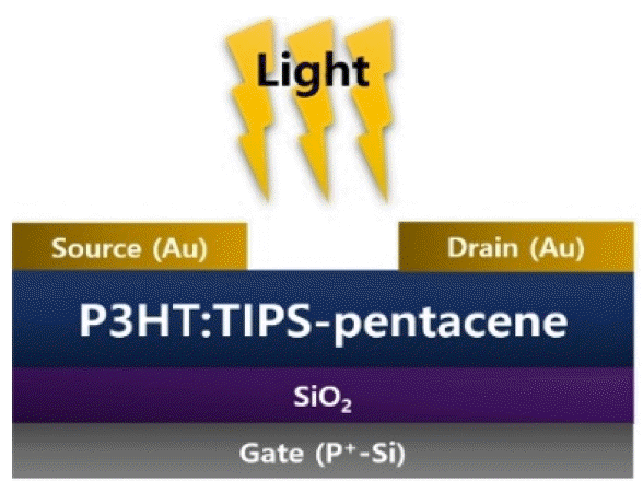
Schematic illustration of P3HT:TIPS-pentacene-blend TFT upon irradiation with light.
To confirm the electrical characteristics of the fabricated TFTs during irradiation with light of specific wavelengths, the TFTs were irradiated with monochromatic light generated by a xenon lamp (450 W). The wavelength of the irradiated light was controlled using a MonoRa-320i monochromator, and the intensities of the irradiated light were measured to be 2.3, 3.9, and 5.1 mW/cm2 at 695, 515, and 450 nm, respectively. The resolution of the monochromatic light source used in this experiment was approximately 8.6 nm. A semiconductor analyzer was used to measure the electrical characteristics of the TFTs in the dark, and upon irradiation.
3. Results and Discussion
The output characteristics of the P3HT, P3HT:TIPS-pentacene blends, and TIPS-pentacene TFTs in the dark are shown in Fig 2(a). In our experiment, the drain voltage (VD) was swept from 0 to -40 V in increments of -1 V at different gate voltages (VG) of 0, -10, and -20 V. The drain current (ID) of all the fabricated TFTs became saturated. On the other hand, the blended TFTs exhibited weaker currents than the pristine devices, that is, the pristine P3HT and TIPS-pentacene TFTs. Figure 2(b) shows the transfer characteristics of the fabricated transistors in the dark with VD fixed at -20 V and VG varying from 15 to -40 V in 1 V steps.

(a) Output (ID versus VD) and (b) transfer (ID versus VG) characteristics of the fabricated TFTs measured in the dark. From left to right: electrical characteristics of the TFTs with the various P3HT:TIPS-pentacene blend ratios of 1:0, 1:0.25, 1:0.5, 1:0.75, and 1:1. The rightmost curves pertain to the pristine TIPS-pentacene TFT.
For the P3HT TFT, both the on-state and off-state currents were high, and in the case of the TIPS-pentacene TFT, high on-state currents and low off-state currents were observed. The blended TFTs had low on-state currents, as confirmed by the output characteristics, but low off-state currents, compared to the P3HT device. Based on these transfer characteristics, the on/off current ratio and field-effect mobility (µ) properties were determined. As observed in Fig 3(a), the blended TFTs had larger on/off ratios than those of the pristine P3HT TFT. Considering that the blended TFTs had lower on-state currents, the observed larger on/off current ratios of the blended TFTs may be due to the greater decrease in the off-state currents, which resulted from the addition of TIPS-pentacene to the P3HT:TIPS-pentacene blended films. At the same time, as shown in Fig 3(b), the blended TFTs possessed lower µ values than the P3HT and TIPS-pentacene TFTs. This may be indicative of the generation of structural defects in the P3HT:TIPS-pentacene blended films.
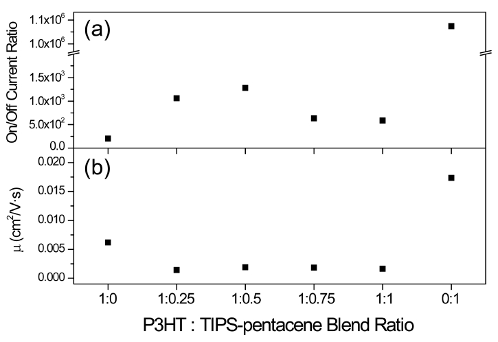
(a) On/off current ratio and (b) μ properties extracted from the transfer characteristics of each of the fabricated TFTs measured in the dark.
It is well known that P3HT molecules prefer to form an amorphous film, whereas TIPS-pentacene molecules form a polycrystalline film. Figure 4 presents illustrations of the surface morphologies of the P3HT, P3HT:TIPS-pentacene blended, and the TIPS-pentacene films. It is assumed that the charge carriers are transported via amorphous polymer chains as well as the crystals that formed in the film, as shown in Fig 4. In the P3HT:TIPS-pentacene blended film, the TIPS-pentacene crystals appeared as islands embedded in the amorphous P3HT matrix. Here, it should be noted that the molecular weight (Mw) of the TIPS-pentacene was 639.07 g/mol, and a small molecule such as this does not experience chain entanglement and hence a high degree of charge-carrier mobility, µ.
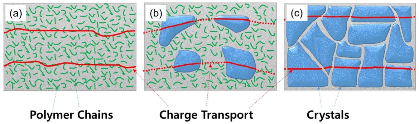
Illustrations of structural constructions and charge transport pathways for the (a) P3HT, (b) P3HT:TIPS-pentacene blended, and (c) TIPS-pentacene films. The short green and red lines represent polymer chains and charge transport pathways, respectively, and the blue pebbles represent TIPS-pentacene crystals.
For the P3HT:TIPS-pentacene blended TFTs, the P3HT with an Mw of 57 kg/mol is thought to reduce the grain width of the TIPS-pentacene, thereby lowering µ due to the formation of defect states at the grain boundaries of the TIPS-pentacene [13,14]. In contrast, it should be noted again that the off-state currents of the P3HT:TIPS-pentacene blended TFTs were relatively lower than those of the P3HT-based TFTs, but higher than those of the TIPS-pentacene-based TFTs. Because of the relatively low ionization potential of P3HT, these molecules undergo oxidation doping by easily forming P3HT–O2 complexes in the film [15,16]. Thus, we consider the formation of complexes to decrease in the blended films because of the presence of TIPS-pentacene. This helps to prevent an increase in the off-state currents in the P3HT:TIPS-pentcene blended TFTs. We suggest that the blended films possess a narrow grain width and a low level of doped oxygen, which explains the low mobility and intermediate level of off-state currents in the blended TFTs.
The absorbance of the P3HT, TIPS-pentacene, and P3HT:TIPS-pentacene blended films was measured by recording their spectra in the wavelength range from 400 to 750 nm, as shown in Fig 5(a). The pristine P3HT film exhibited maximum absorbance at approximately 515 nm, whereas the highest intensity peak of the pristine TIPS-pentacene film was detected at approximately 450 nm. The P3HT:TIPS-pentacene blended film exhibited characteristic peaks at both 515 and 450 nm, due to the combined effects of the P3HT and TIPS-pentacene materials. Figure 5(b) shows that the energy band gap (EG) properties of the TIPS-pentacene and P3HT were 1.87 and 2.0 eV, respectively [17-19].
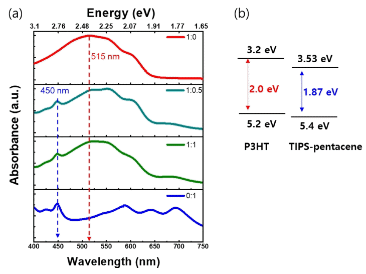
(a) Absorbance spectra of P3HT:TIPS-pentacene blended thin films for the wavelength range of 400 to 750 nm. From top to bottom, pristine P3HT at 1:0 ratio, blends of 1:0.5 and 1:1, pristine TIPS-pentacene at 0:1 ratio. (b) Energy band diagrams of P3HT and TIPS-pentacene.
Based on the observed optical characteristics, the electrical properties of the fabricated TFTs were then analyzed under incident light at wavelengths of 515 and 450 nm to clarify how the irradiation influenced the electrical characteristics of the TFTs. Figure 6 shows the transfer characteristics of the TFTs fabricated with various P3HT:TIPS-pentacene blend ratios, which were measured under light irradiation conditions. For the measurement, VD was fixed at -20 V and VG was varied from 15 to -40 V in 1 V steps. Figure 7 compares the light-to-dark current ratio of the fabricated TFTs when exposed to monochromatic light of different wavelengths; the light-to-dark current ratio properties were extracted from the transfer characteristics of the transistors shown in Fig 6. In addition, a drain voltage of -20 V and gate voltage of 15 V were applied to measure the off-state currents of the TFT, while a drain voltage of -20 V and gate voltage of -40 V were applied to measure the on-state currents.
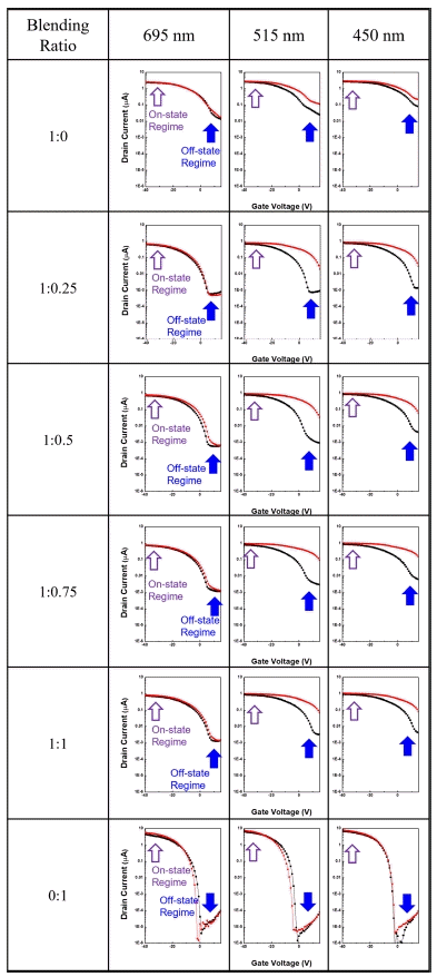
Transfer characteristics of the fabricated TFTs according to the P3HT:TIPS-pentacene blending ratio under light irradiation conditions.
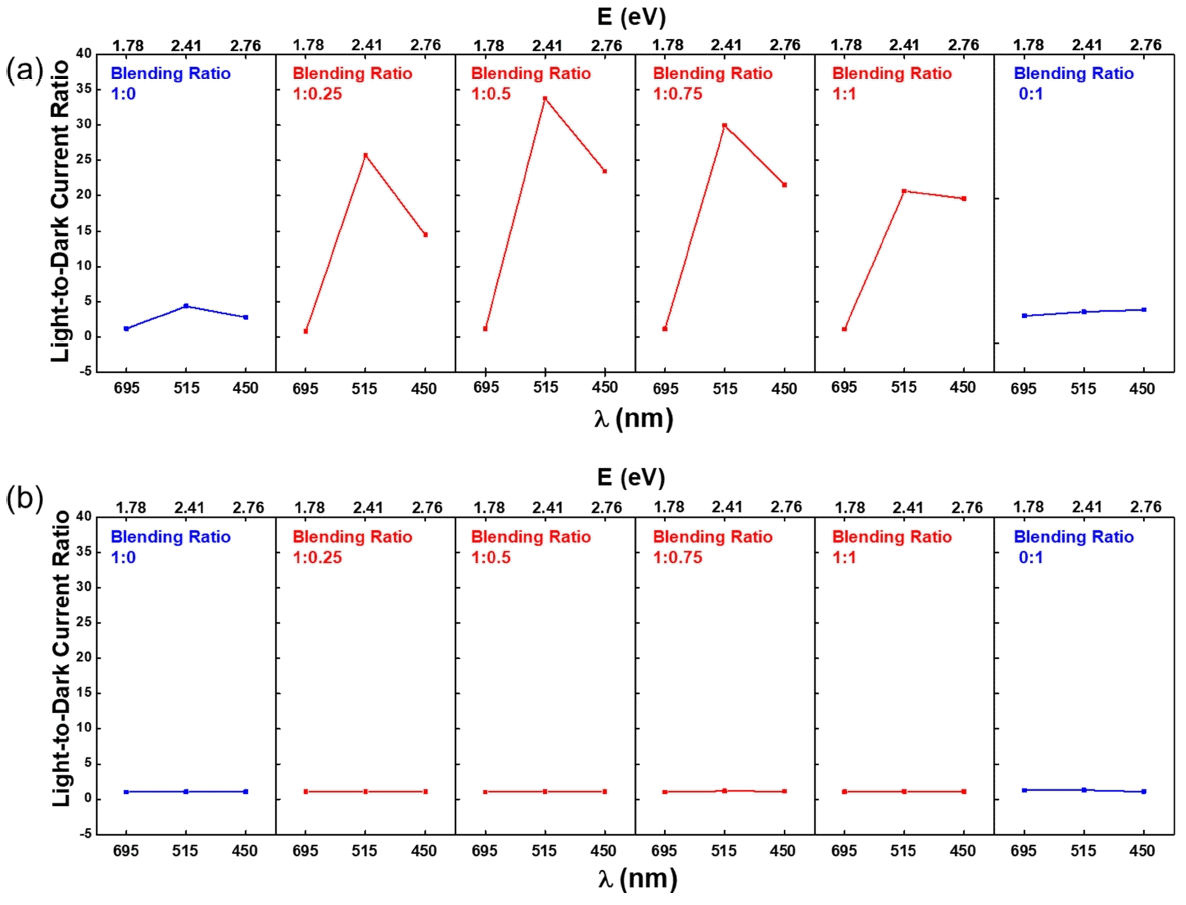
Light-to-dark current ratios extracted from the transfer characteristics of TFTs in (a) off-state and (b) on-state regime.
In this experiment, monochromatic light with a wavelength of 695 nm was used to evaluate the dark current of the transistor, and the light-to-dark current ratio was obtained by dividing the photo-induced current by the dark current. Note that the light-to-dark current ratio is useful for evaluating the amplification of currents under light irradiation. As shown in Fig 7, all of the transistors exhibited negligible changes in current when irradiated with light with a wavelength of 695 nm. The EG values of P3HT and TIPS-pentacene were 2.0 and 1.87 eV, respectively, which correspond to wavelengths of 622 and 663 nm. Thus, the optical energy of monochromatic light with a wavelength of 695 nm is not sufficient to generate excitons in the P3HT, TIPS:-pentacene, and the P3HT:TIPS-pentacene blended films. This confirms that monochromatic light with a wavelength of 695 nm can be used to evaluate the dark current of the fabricated TFTs in this study.
An important observation from Fig 7(a) is that the light-todark current ratio of the blended TFTs significantly improved compared to the pristine P3HT and TIPS-pentacene TFTs. Among our results, the blended TFT with the P3HT:TIPS-pentacene blending ratio of 1:0.5 had the largest light-to-dark current ratio, i.e., approximately 33.8 upon irradiation with 515 nm light and approximately 23.5 when irradiated with monochromatic light with a wavelength of 450 nm. Compared to the case with 450 nm irradiation, the blended TFTs had a larger current ratio when irradiated at 515 nm. This is because the P3HT:TIPS-pentacene blended films absorb more strongly at 515 nm, as shown in Fig 5. Simultaneously, the light-induced amplification of the onstate currents was negligible because the field-induced charges dominated the photogenerated charges in the TFTs, as shown in Fig 7(b).
Considering the notable influence of light irradiation on the off-state currents of the fabricated TFTs, the photosensitivity, P, of each device was extracted from the transfer characteristics in the off-state regime. The photosensitivity of phototransistors is normally used to analyze the amount of photo-induced charges in TFTs upon exposure to light. Figure 8 shows the P values, which were measured by irradiating the fabricated TFTs with monochromatic light of 515 and 450 nm. This represents the pure photocurrent and excludes the current under dark conditions, that is, noise. P can be expressed as follows:
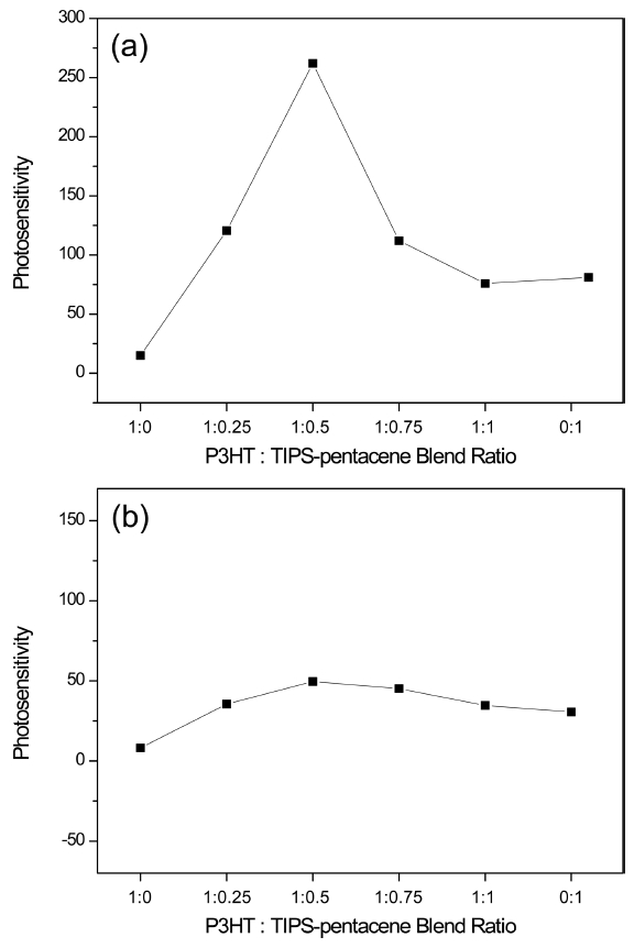
Plots of P versus P3HT:TIPS-pentacene blend ratio upon irradiation with light at wavelengths of (a) 515 nm and (b) 450 nm.
where IPh is the photo-induced ID; IDlight and IDdark are ID under light and dark conditions, respectively [20]. The P value for each case was the average of measurements of 10 or more devices. As shown in Fig 8(a), upon irradiation at 515 nm, the blended TFT with a P3HT:TIPS-pentacene blending ratio of 1:0.5 exhibited the largest P of 261.9, which was more than 17 times larger than that of the pristine P3HT TFT (14.9). Similarly, when irradiated with monochromatic light of 450 nm, the blended TFT with a P3HT:TIPS-pentacene blending ratio of 1:0.5 also exhibited the largest P of approximately 49.6, as shown in Fig 8(b). The larger P at 515 nm is considered to possibly be related to the light absorption characteristics of the P3HT:TIPS-pentacene blended films, as shown in Fig 5.
Figure 9 shows images of the surfaces of the pristine P3HT film and P3HT:TIPS-pentacene blend films with blending ratios of 1:0.5 and 1:1, captured using scanning electron microscopy (SEM). The pristine P3HT film had a relatively uniform distribution and shape, whereas crystals appeared on the surface of the film when TIPS-pentacene was added. Additionally, the specific gravity was much higher for the 1:1 mixing ratio, as shown by the mixed film with a ratio of 1:0.5.
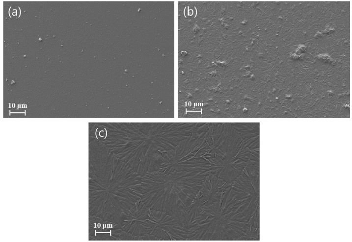
SEM images of (a) pristine P3HT film and P3HT:TIPSpentacene blend films with blending ratios of (b) 1:0.5 and (c) 1:1.
In P3HT, charge carriers propagate by hopping through each state of the amorphous film, whereas in TIPSpentacene, they propagate rapidly within the crystal and are captured and released at the grain boundaries. When the P3HT generates an exciton pair upon irradiation with monochromatic light at 515 nm, electrons may fill the positively charged states in the film, and the holes can be transferred to the TIPS-pentacene. The transitioned holes propagate rapidly along the crystals of the TIPS-pentacene, thereby increasing the photocurrent. Consequently, some of the exciton pairs generated in the P3HT:TIPS-pentacene blended film can fill the trapped states, whereas others can contribute to the photocurrent of the TFTs. Polymer chains also function as interconnecting pathways between crystal regions. This suppresses the trapping behavior of the charge carriers and thus facilitates the transport of photogenerated excitons.
As observed in the surface structure of the 1:0.5 blend film, when P3HT polymer fills the gap between the TIPSpentacene crystals, the photoexcited charge carriers can be output as photocurrents without being trapped at the TIPS-pentacene crystal boundary. That is, in the blended film with strong TIPS-pentacene crystallinity, the TIPS-pentacene crystal boundary possibly serves as a trapping site for photoexcited charge carriers. For this reason, it is understood that when using the 1:0.5 blend film with a higher relative ratio of P3HT, more P3HT polymers can fill the TIPS-pentacene boundary, resulting in greater photosensitivity. Accordingly, with a P3HT:TIPS-pentacene blend ratio of 1:0.5, the P value of the blended TFT was enhanced upon irradiation with light at 515 and 450 nm. The experimental results therefore demonstrate that the optical response characteristics of a transistor can be improved by blending heterogeneous semiconductor materials.
4. Conclusions
In this study, we investigated the electrical characteristics of P3HT:TIPS-pentacene blended TFTs while they were being irradiated with light to analyze the correlation between the light absorbance and electrical properties of the heterogeneously blended organic semiconductors. The light-to-dark current ratio was significantly larger and the photosensitivity properties of the P3HT:TIPS-pentacene blended TFTs were significantly superior to those of the pristine P3HT and TIPS-pentacene TFTs.
In particular, these improvements were more pronounced when the TFTs were irradiated with 515 nm light, because the P3HT:TIPS-pentacene blended films absorb more strongly at 515 nm. These results demonstrate that the exciton pairs generated at specific wavelengths were compatible with the absorption characteristics of the material, and that the characteristics of the respective component materials can be integrated into the blended TFTs. We expect the use of blended heterogeneous semiconductor materials to pave the way to effective organic TFTs with selective optical response for application in advanced optoelectronic systems. Future research is required to analyze the transport processes of excitons generated between the heterogeneous semiconductor materials.
Acknowledgements
This research was supported by Basic Science Research Program through the National Research Foundation of Korea (NRF) funded by the Ministry of Education (NRF-2021R1A6A3A01088460).