Electrospun Nanofiber-Based Electrodes Composed of Core-Shell (PVDF)-(Al) Structures for Application to Flexible Electronics
Article information
Abstract
Nanostructured transparent conductors have been studied intensively for application to flexible and transparent electronic devices. Among diverse nanomaterials, electrospun nanofibers provide several advantages over other nanomaterials, including a high aspect ratio, uniform distribution, and a facile fabrication process. In the present study, an electrode composed of a core-shell (PVDF)-(Al) structured nanofiber mesh film was fabricated via electrospinning and sputtering processes, without any high-temperature heat treatment or wet chemical treatment. A free-standing circular collector was used to form a PVDF nanofiber mesh film, to perform the conformal coating of Al onto the PVDF surfaces. The parameters of the tip-to-collector distance and the electrospinning voltage needed to stably form a PVDF nanofiber mesh film were determined. The sheet resistance of the mesh film was dramatically reduced from 1870 Ω/sq. to 154 Ω/sq. when the sputtering time was increased from 2 min to 4 min, an outcome explained by the changed surface morphology of the Al coating layer. The sheet resistance decreased from 657 Ω/sq. to 15.4 Ω/sq. with an increase in the electrospinning time from 2 min to 8 min due to the increased numbers of nanofibers and junctions. When the transmittance at 550 nm with respect to the sheet resistance was plotted for these mesh films, the graph was divided into the bulk and percolation regimes. Mesh films with transmittance rates that exceeded 85% exhibited sheet resistance that clearly increased with an increase in transmittance, indicating a percolation network. Finally, the durability of the core-shell (PVDF)-(Al) structured nanofiber mesh film was evaluated using a repetitive bending test, the results of which clearly showed superior performance over Al thin film. With inexpensive metal Al, a competitive flexible and transparent electrode was fabricated in the form of a core-shell (PVDF)-(Al) structured nanofiber mesh film.
1. INTRODUCTION
Given recent advances in flexible transparent electronic devices, creating high-quality transparent conducting electrodes (TCEs) has become increasingly important. To date, TCEs have been applied in a range of electronics, such as light-emitting devices [1,2], solar cells [3], touchscreens [4], and heaters [5]. The important properties of TCEs are the sheet resistance (Rs) and transmittance (T), and the particular qualities required differ depending on the electronic device to which they are applied. For example, the TCEs used in resistive touchscreen panels require a sheet resistance of (Rs <500 Ω/sq.) and transmittance of (T>80%), whereas a lower sheet resistance (1−50 Ω/sq.) and higher transmittance (T>90%) are required for those used in organic light-emitting diodes [6,7]. In addition to these two properties, the mechanical strength and manufacturing cost are also important considerations for TCEs. Indium tin oxide (ITO) is one of the most widely used materials for TCEs due to its high transmittance (T>90%)[8]. However, ITO is expensive because of the low abundance of indium, and ITO film is vulnerable to breaking when bent given its brittleness [9].
To overcome the constraints of ITO films, transparent electrodes have been developed with various materials and structures, including carbon nanotubes (CNTs) [10], graphene [11,12], metal nanowires [13,14], metal nanofibers [15,16], and metal nanotroughs [5,17]. Some of these transparent electrodes have their own limitations which must be addressed before they can serve as alternative electrodes for ITO film. For example, transparent electrodes based on graphene have low sheet resistance and high transparency (~20 Ω/sq. at 90% transmittance) [11]. However, they require high-temperature heat treatment, at 1000 °C, and their high processing cost hinders their use as a transparent conducting electrode [4]. On the other hand, electrodes based on metal nanowires are known for superior conductivity and transmittance. They exhibit a sheet resistance of 8 Ω/sq. at >80% transmittance and excellent mechanical durability [14]. However, fabrication processes to minimize the contact resistance at the nanowire junctions tend to be complicated [13].
As a way of simplifying the complicated fabrication process, TCEs based on electrospun nanofibers have attracted significant attention. Electrospinning provides several advantages during the fabrication process of transparent electrodes. For example, the properties of the nanofiber can easily be adjusted by changing certain fabrication conditions, such as the voltage and tip-to-collector distance (TCD) [18]. Furthermore, the nanofiber assemblies can be facilely controlled according to the type of collector used. TCEs based on electrospun nanofibers exhibit superior transparency and conductivity, as well as mechanical flexibility [5,17]. However, it is essential to remove the electrospun polymer nanofibers used as a template. A chemical treatment is required during this process, and as a result, the fabrication process is still complicated.
In the present study, we fabricated a core-shell (PVDF)-(Al) structured nanofiber mesh film as a transparent electrode. There are several metals more electrically conductive than Al, however, Al was chosen as a conducting material because of its low cost compared to other metals such as Pt, Ag, and Cu. Cost is an important criterion particularly when the electrode is used in a large scale wearable device.
One of the greatest advantages of this novel TCE is its simple fabrication process, consisting of only electrospinning and sputtering. Since the entire process can be performed without a high-temperature environment, the TCEs in this study can be deposited onto a wide range of substrates. In addition, the sheet resistance, transparency, and mechanical durability of the electrodes are similar to or superior to those of the TCEs introduced earlier.
In this study, we show that the properties of the proposed transparent electrode, specifically the transparency and conductivity, can be facilely controlled during the electrospinning process. Furthermore, the proposed fabrication process provides a high degree of freedom with regard to the types of coating metals and substrates used.
2. EXPERIMENTAL METHODS
Polyvinylidene fluoride (PVDF) powder (Sigma Aldrich, Mw ~534,000) was used to prepare the solution for the electrospinning process. The solvent was a mixture of 7 ml of acetone (Duksan Reagents) and 3 ml of dimethyl formamide (DMF, Duksan Reagents). The concentration of the PVDF solution was 15 wt%, and it was prepared by dissolving 8.5 g of solvent and 1.5 g of PVDF powder at 300 RPM and 100 °C for 1 h using a magnetic stirring method. Thereafter, the solution was cooled at room temperature for 20 min and then transferred to a 10 ml syringe (HENKE-JECT) for the electrospinning process. Electrospinning was performed using an electrospinning/spray system (ESR200, NanoNC) and was typically conducted at a 17 cm TCD, at 10 kV voltage and with a 40 μL/min solution flow rate. In the present fabrication process, a free-standing nanofiber network was prepared so that it could be facilely transferred to diverse substrates [17]. A schematic illustrating the fabrication process of the freestanding PVDF nanofiber mesh film is shown in Fig 1(a). PVDF was chosen as the core material because PVDF nanofibers have excellent flexibility under external mechanical movement [19]. In this work, a circular collector made of stainless steel with an inner diameter of 37 mm was used to produce randomly oriented PVDF nanofibers [20]. The collector was placed 2 cm above the floor to prevent the nanofibers from sticking to the bottom floor. The density of the PVDF nanofiber mesh film was facilely controlled during the electrospinning process.

Schematic illustrating the fabrication process of the core-shell (PVDF)-(Al) structured nanofiber mesh film: (a) fabrication of randomly aligned PVDF nanofibers on a circular collector using an electrospinning technique, (b) evaporation of the solvent at 100 °C using a vacuum oven, (c) Al thin film deposition on the surface of PVDF nanofibers via DC sputtering, (d) transferal of the core-shell (PVDF)-(Al) structured nanofiber mesh film onto a PDMS substrate, and (e) the completed flexible and transparent electrode on a PDMS substrate.
The fabricated PVDF nanofiber mesh film was subsequently baked for 2 h at 100 °C using an oven (SHVDO-30NH, Samheung Energy) to remove any residual solvent (Fig 1(b)). Thereafter, Al was deposited onto the surfaces of the electrospun PVDF nanofibers by means of DC magnetron sputtering (KVS-2000, Korea Vacuum Tech.) with an Al sputter target (99.999% purity, RND Korea) (Fig 1(c)). The base pressure inside the sputter chamber was 2×10⁻⁵ Torr, and the sputtering process was carried out at a power of 150 W at a working pressure of 5 mTorr in Ar gas. Sputtering is advantageous compared to other thin film deposition techniques in that it enables a conformal Al coating onto the surface of PVDF nanofibers and does not require a high-temperature environment. Subsequently, the core-shell (PVDF)-(Al) structured nanofiber mesh film was transferred onto a polydimethylsiloxane (PDMS) substrate to measure its sheet resistance and transmittance (Fig 1(d)).
The morphology of the core-shell (PVDF)-(Al) structured nanofiber mesh films was observed using a scanning electron microscope (SEM, JSM-6700F, JEOL Ltd.). An atomic force microscope (AFM, XE-150, Park Systems) was used to observe the topography of the electrode surfaces more precisely [21,22]. For stable AFM measurements, an ElectriCont-G AFM probe with a 0.2 N/m spring constant was used at a scan rate of 0.5 Hz. In particular, the conductivity of an individual nanofiber was measured using a conductive AFM (C-AFM) with a tip bias of 4 mV.
The sheet resistance was measured using the four-point probe method (M4P302, MSTECH) and a source measure unit (SMU, Model 2612B, Keithley). During four-point probe measurements, current was applied to the sample through the two outer probes and voltage was measured using the two inner probes. The sheet resistance was obtained by multiplying the computed resistance with the correction factor 4.532 [23]. To measure the optical transparency in the visible wavelength range, a UV-vis spectrophotometer (Specord 200 Plus, Analytik Jena) was used. Finally, the durability of the electrode under mechanical stress was evaluated using a bending tester (JIBT-200, Junil Tech.).
3. RESULTS AND DISCUSSION
Figs 2(a)–2(e) show the various transparency rates of the core-shell (PVDF)-(Al) structured nanofiber mesh films depending on electrospinning times. It should be noted that the sputtering time was constant at 5 min. It can be clearly observed that the transparency of the electrode gradually degraded as the density of the nanofibers was increased. Fig 2(f) shows a SEM image of the electrode prepared by electrospinning for 8 min, corresponding to Fig 2(a). It can be confirmed that in spite of the high transparency a number of nanofibers can actually be observed via the naked eye. The empty space in Fig 2(f) was confirmed to amount to 76.3% using ImageJ software.
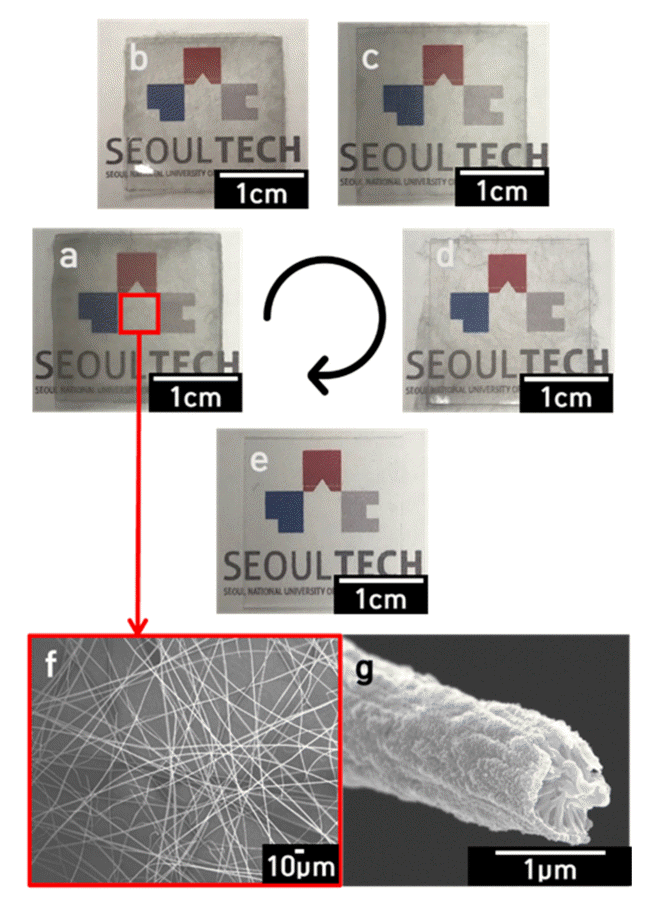
Transparency of the core-shell (PVDF)-(Al) structured nanofiber mesh films: (a) digital photos showing the transparency outcomes of the core-shell (PVDF)-(Al) structured nanofiber mesh films with electrospinning times of 8 min, (b) 6 min, (c) 4 min, (d) 2 min, and (e) 0 min (in the absence of nanofiber); (f) SEM image of the core-shell (PVDF)-(Al) structured nanofiber mesh film, and (g) SEM image of a single core-shell (PVDF)-(Al) structured nanofiber.
Fig 2(g) shows the cross-section of the core-shell (PVDF)-(Al) structured nanofiber, illustrating the conformal deposition of the Al thin film on the surface of the PVDF nanofiber. Sputtering was chosen as the thin film deposition method because under sufficiently high pressure Al atoms can approach the substrate at a wide range of angles. In contrast, during evaporation Al vapor travels only in a straight line, so it would have not reached to the bottom of the PVDF nanofibers. It is noted that the uniformity of the Al layer can be further improved by conducting a second Al sputtering on the flipped PVDF nanofiber mesh film when a higher uniformity of Al layer is required.
Fig 3 shows the energy-dispersive X-ray spectroscopy (EDS) analysis of PVDF nanofibers and Al-coated PVDF nanofibers. First of all, in Fig 3(a) the dense distribution of the elements C and F are matched to the locations of the PVDF nanofibers. The Si and Pt peaks in the EDS spectra (Fig 3(b)) originate from the PDMS substrate and coating layer used to prevent surface charging during the measurement, respectively. A strong Al peak as well as C and F peaks were detected in the EDS spectra of the Al-coated PVDF nanofiber, indicating the core-shell (PVDF)-(Al) structures.
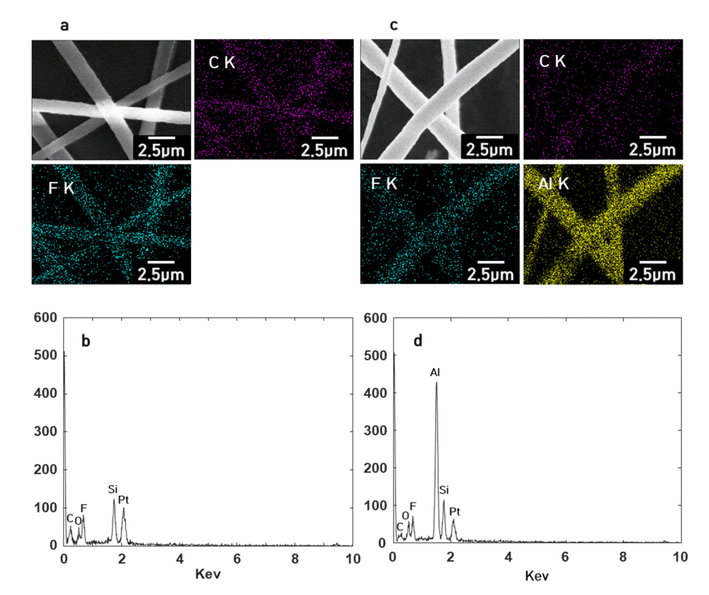
Energy-dispersive X-ray spectroscopy (EDS) analysis of PVDF nanofibers and Al coated PVDF nanofibers. (a) SEM image and EDS maps, and (b) EDS spectra of the PVDF nanofibers. (c) SEM image and EDS maps, and (d) EDS spectra of the Al coated PVDF nanofibers.
The morphology and conductivity of an individual nanofiber were measured using AFM and C-AFM, respectively. The diameter of the nanofiber shown in Fig 4(a) was approximately 1.7 μm, greater than that in the SEM image (Fig 2(g)). This error originates from the finite response time of the AFM feedback circuit and the contact between the AFM tip sidewalls and the nanofiber. The surface roughness of the Al thin film depicted in the SEM image (Fig 2(g)) can also be observed in the 2D and 3D topography images (Figs 4(a)–(b)). The current map (Fig 4(c)) clearly indicates the highly conductive core-shell (PVDF)-(metal) structured nanofiber, in contrast to the insulating PDMS substrate.
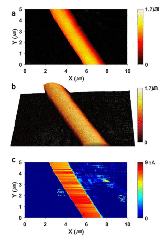
Local topography and current maps for the single core-shell (PVDF)-(Al) structured nanofiber measured by AFM and C-AFM: (a) 2D topography, (b) 3D topography, and (c) 2D current map.
The formation of a PVDF nanofiber mesh film on a free-standing circular collector requires more constrained electrospinning conditions than that on an ordinary flat substrate. In particular, depending on the TCD and voltage during the electrospinning process, the PVDF nanofibers may not be formed within the circular collector. Fig 5(a) presents a map of the electrospinning conditions associated with the TCD and voltage for a free-standing circular collector with an inner diameter of 37 mm and a 15 wt% PVDF solution [24]. In Fig 5, the conditions of the nanofiber mesh films are classified with four Greek characters (α , β, γ, and δ). First, the red area (α) in the map indicates an occasion where the liquid jet was not formed properly because the applied voltage was relatively low for the given TCDs. In this case, whipping did not occur, and the solution fell from the needle in the form of drops.
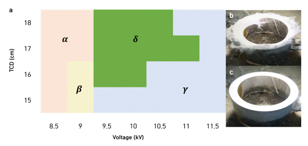
(a) Map of the electrospinning conditions for the growth of the PVDF nanofiber mesh film inside the circular collector; (b) and (c) are the resultant PVDF nanofibers under the electrospinning conditions in the yellow area β and the blue area γ, respectively.
In the yellow (β) and blue regions (γ), nanofibers were generated but were not properly formed inside the circular collector. The yellow area (β) indicates a case in which nanofibers were produced but whipping did not properly occur due to the insufficient voltage. Thus, thick nanofibers were produced. Additionally, the electric force between the PVDF nanofibers was stronger than the applied electric field, with some nanofibers even forming outside of the circular collector as a result (Fig 5(b)). Meanwhile, within sufficient voltage and TCD ranges, whipping occurred, stably producing PVDF nanofibers. However, in these instances, the electric field was much stronger than the electric force between the PVDF nanofibers and a mesh film did not therefore form in the empty space inside the circular collector. This corresponds to the blue area (γ). Under these TCD and voltage conditions, the nanofibers accumulated only on the surface of the circular collector or the pedestal due to the excessively strong electric field (Fig 5(c)).
To form a PVDF nanofiber mesh film inside the circular collector, the optimal condition of electrospinning corresponds to the green area (δ). In the beginning, the nanofiber mesh film tended to grow from the surface of the circular collector, gradually expanding toward the center of the collector. Under these TCD and voltage conditions, it took 2 – 3 min to complete the formation of the nanofiber mesh film.
Fig 6 shows the widths of the core-shell (PVDF)-(Al) structured nanofibers with respect to the sputtering time as measured from the SEM images. With an increase in sputtering time from 2 to 10 min, the width of the nanofiber increased from 1.17 μm to 1.68 μm. The relationship between the nanofiber width and sputtering time was approximately linear, and the average growth rate of the Al thin film thickness was approximately 32 nm/min.

Widths of the core-shell (PVDF)-(Al) structured nanofibers with respect to the sputtering time; the relationship between the width and sputtering time was approximately linear with an Al thin film growth rate of 32 nm/min.
In this core-shell (PVDF)-(Al) structured nanofiber mesh film, the sheet resistance can be facilely controlled during the fabrication process. Figs 7(a) and 7(b) represent the sheet resistance with respect to the sputtering time and the electrospinning time, respectively. As shown in Fig 7(a), the sheet resistance decreased continuously from 1870 Ω/sq. to 22.9 Ω/sq. when the sputtering time was increased from 2 min to 10 min. During these measurements, the electrospinning time was constant at 6 min. It is interesting to note that there was a noticeable drop in the sheet resistance when the sputtering time was increased from 2 min to 4 min, most likely stemming from the different surface morphologies of the Al-coated PVDF nanofibers.
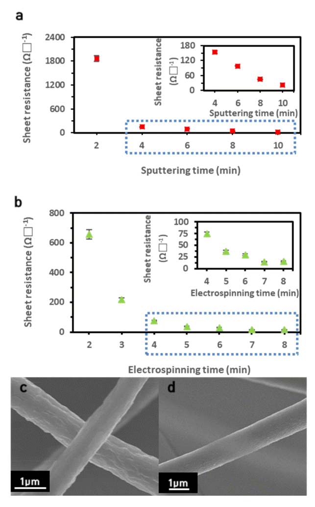
(a) Sheet resistance of the core-shell (PVDF)-(Al) structured mesh film with respect to the sputtering time, (b) sheet resistance with respect to the electrospinning time, and (c) a SEM image of an Al-coated PVDF nanofiber after sputtering for 2 min and (d) 4 min
Figs 7(c) and 7(d) show SEM images of Al-coated PVDF nanofibers after 2 min and 4 min of sputtering, respectively. In Fig 7(c), the rough surface of the PVDF nanofibers, originating from the porous PVDF, is visible due to the thin Al layer. However, in Fig 7(d), the Al layer is sufficiently thick, producing a smooth surface on the Al-coated PVDF nanofiber. Therefore, during this fabrication process, an Al sputtering time exceeding 4 min is essential to form an Al thin film sufficient to decrease the sheet resistance.
Meanwhile, the sheet resistance of the mesh film decreased from 657 Ω/sq. to 15.4 Ω/sq. with an increase in the electrospinning time from 2 min to 8 min. The sputtering time was held constant at 10 min. The increased electrospinning time resulted in an increased number of junctions as well as nanofibers in the mesh film. Thus, the decrease in sheet resistance can be explained by the increased numbers of nanofibers and junctions. It should be noted that in this core-shell (PVDF)-(Al) structured nanofiber mesh film, the junction resistance between the nanofibers should be sufficiently small as the Al thin film was directly deposited onto these junctions. Finally, the sheet resistance was no longer reduced when the electrospinning time exceeded 7 min.
Meanwhile, to evaluate the transparency of the core-shell (PVDF)-(Al) structured nanofiber mesh film, the optical transmittance was measured in a wavelength range from 400 – 1000 nm. As shown in Fig 8(a), the optical transmittance at a wavelength of 550 nm decreased from 92.4% to 73.9% as the electrospinning time was increased from 2 min to 10 min. For these nanofiber mesh films, percolation theory was applied to evaluate their performance as a transparent electrode. The transmittance at 550 nm with respect to the sheet resistance of the nanofiber mesh films formed with various electrospinning times is shown in Fig 8(b). The resultant plot is clearly divided into two regimes, in this case, bulk and percolation regimes.

(a) Transmittance of the core-shell (PVDF)-(Al) structured nanofiber mesh film in the 400-1000 wavelength range for various electrospinning times, (b) transmittance at a wavelength of 550 nm with respect to the sheet resistance, and (c) log (T0.5-1) with respect to log(Rs/Z0).
In earlier work, the relationship between the sheet resistance and the transmittance in a percolation network was described by the following equation [25–27]:
where Π, n, Z0, and Rs indicate the percolation figure of merit, the percolation exponent, the impedance of free space (377Ω), and the sheet resistance, respectively. According to Fig 8(b), when the transmittance at 550 nm surpasses approximately 85%, the core-shell (PVDF)-(Al) structured nanofiber mesh film follows percolation theory via Eq. (1). By substituting the data in Fig 8(b) into Eq. (1), and n were determined to be 21.8 and 1.22, respectively. In general, superior transparent conductors with high T and low Rs values favor a large and a small n [27].
When compared to the and n values of previously developed TCEs with a percolation network, the core-shell (PVDF)-(Al) structured nanofiber mesh film showed considerable competitiveness [26,27].
Meanwhile, for the core-shell (PVDF)-(Al) structured nanofiber mesh films, log (T0.5-1) is presented with respect to log (Rs/Z0) in Fig 8(c). The plot clearly indicates that the mesh films fabricated by electrospinning for 2 – 7 min follow Eq. (1). It is noted that in the bulk regime conductivity is independent of film thickness. In contrast, in the percolative regime, as the number of conducting paths increases, the film conductivity increases until it reaches the conductivity of bulk materials [27].
To assess the durability of the core-shell (PVDF)-(Al) structured nanofiber mesh film against repetitive bending and releasing, a bending test was conducted. Fig 9(b) shows the experimental setup, showing a guide that was additionally installed to precisely create a 6 mm bending radius. The bending test was performed at a frequency of 0.5 Hz. The test sample was prepared by electrospinning PVDF nanofibers for 7 min, with this step was followed by sputtering Al for 8 min. The durability of the mesh film during the bending test was compared with that of an Al thin film. The Al thin film sample was prepared via an 8 min sputtering process. Finally, to prevent damage caused by physical contact between the guide of the fixed shaft and the mesh film, the mesh film was protected by a PDMS encapsulation layer.
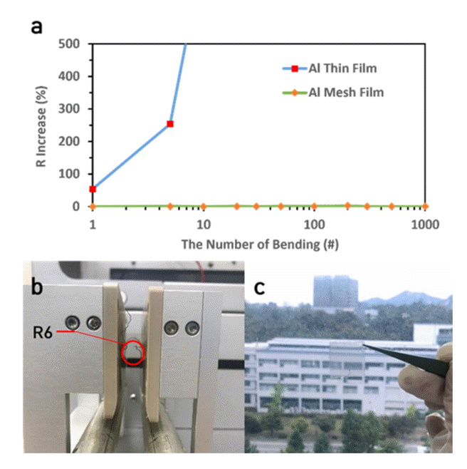
(a) The increase in R of the core-shell (PVDF)-(Al) structured nanofiber mesh film with respect to the number of bending cycles, (b) the experimental setup for the bending test of the mesh film encapsulated by PDMS, and (c) the transparency of the core-shell (PVDF)-(Al) structured mesh film encapsulated by PDMS used in the actual bending test. In (b), the bending radius was 6 mm.
The initially measured sheet resistances of the Al thin film and Al nanofiber were 23.3 Ω/sq. and 259.8 Ω/sq., respectively. However, as shown in Fig 9(a), the resistance (R) of the Al thin film increased by 54% after a single cycle of bending and releasing. After five cycles, the resistance increased by 254%. In contrast, the resistance (R) of the core-shell (PVDF)-(Al) structured nanofiber mesh film increased by only 2.73% during 1000 bending and release cycles. This result indicates that the mesh film has superior durability under mechanical stress compared to an Al thin film. Fig 9(c) illustrates the transparency of the mesh film encapsulated by PDMS that was used in the bending test.
4. CONCLUSIONS
In this study, core-shell (PVDF)-(Al) structured nanofiber mesh films were fabricated for application as a flexible and transparent electrode. A free-stranding circular collector was used to ensure a simple fabrication process, composed of only electrospinning and sputtering. The surface morphology and electrical conductivity of a single PVDF nanofiber coated by Al thin film were characterized by SEM and C-AFM techniques, respectively. The specific TCD and electrospinning voltage conditions for the stable formation of the PVDF nanofiber mesh film were identified. With an increase in sputtering time, the thickness of the Al layer increased at a growth rate of 32 nm/min. A minimum sputtering time of 4 min was required to ensure a sufficient coating of the Al layer on the PVDF nanofibers, which was confirmed by the significantly reduced sheet resistance. The sheet resistance of the mesh film also decreased from 657 Ω/sq. to 15.4 Ω/sq. as the electrospinning time was increased from 2 min to 8 min. Depending on electrospinning time, the relationship between the transmittance and the sheet resistance was either in the bulk or the percolation regime. At more than 85% transmittance, the mesh films exhibited a percolation network. The flexibility of the mesh film was evaluated via a repetitive bending test. The resistance of the mesh film increased by only 2.73% during 1000 bending and release cycles. We demonstrated that the fabricated mesh film based on inexpensive Al can be used as a competitive flexible and transparent electrode.
Acknowledgements
This study was supported by the Research Program funded by the SeoulTech (Seoul National University of Science and Technology).