Effects of V Alloying on Thermoelectric Properties of NbFeSb Half-Heusler Materials Codoped with Ti, Zr, and Sn
Article information
Abstract
NbFeSb-based alloys are promising p-type half-Heusler materials with excellent thermoelectric performance, thermal stability, and naturally abundant constituent elements. Alloying and doping are powerful techniques for enhancing the thermoelectric properties of half-Heusler materials. This study experimentally investigated the effects of V alloying in NbFeSb codoped with Ti, Zr, and Sn. As the V content increases, the electrical conductivity of Nb0.8−xVxTi0.15Zr0.05FeSb0.98Sn0.02 (x = 0, 0.05, 0.1, 0.2, and 0.3) decreases monotonically because of a simultaneous reduction in carrier concentration and mobility, reducing the power factor up to −39% from 4.13 (x = 0) to 2.52 mW m−1K−2 (x = 0.3) at 298 K. Moreover, the lattice thermal conductivity decreases with increasing x; by as much as −40% at the maximum V content of x = 0.3, demonstrating that V addition considerably enhances phonon scattering even in the presence of substitutional dopants Ti, Zr, and Sn. The differences in the mass and size of V and Nb atoms cause a substantial decrease in lattice thermal conductivity. According to our study, the addition of a small V content to Hf-free NbFeSb-based alloys can improve their thermoelectric properties, and a maximum dimensionless figure of merit zT of 0.89 was obtained in Nb0.75V0.05Ti0.15Zr0.05Sn0.98Sb0.02 at 973 K.
1. INTRODUCTION
Thermoelectric devices have distinct features such as noiseless operation, small volume, and longterm reliability. The recent interest in ecofriendly power sources is inspiring research on waste heat recovery via thermoelectric generation. Among the promising thermoelectric materials for mid-to-high temperature applications, including skutterudites [1-3] and silicides [4-6], half-Heusler (HH) materials have attracted considerable attention because they show major advantages, such as high performance, mechanical robustness, and thermal stability [7-9]. NbFeSb-based HH compounds have recently been intensively investigated, and improved thermoelectric performances (TEPs) have been observed in the materials doped with Ti [10-12] and Hf [13,14]. The relative abundance of the constituent elements in the earth’s crust makes NbFeSb-based materials very promising because of their low cost and mass production compatibility.
Recently, the TEP of NbFeSb-based materials has been considerably enhanced using the “diagonal-rule” doping technique, achieving a maximum figure of merit (zTmax) of ~1.5 at 1200 K for Nb1−xHfxFeSb [13]. Ti doping of NbFeSb provided the first breakthrough of TEP enhancement, resulting in a 25% increase in power factor for Nb0.6Ti0.4FeSb0.95Sn0.05 [10]. Further optimization of the sintering temperature yielded a massive power factor of 106 μW cm−1 K−2 at 300 K for Nb0.95Ti0.05FeSb and a high maximum zT of 1.1 at 973 K for Nb0.8Ti0.2FeSb [12]. These major achievements proved that Hf and Ti are excellent p-type dopants for NbFeSb. One of their secondary functions is to decrease lattice thermal conductivity (κlat) by enhancing phonon scattering [11-14]. Among the p-type dopants (Hf, Ti, and Zr), Hf exhibited the best advantages for TEP enhancement [15,16]; however, its rarity and high cost limit its practical applications.
Another traditional strategy used for band engineering and the suppression of thermal conductivity is alloying NbFeSb with isoelectronic elements. Fu et al. investigated the substitution of V with Nb in VFeSb and reported a 55% reduction in the thermal conductivity of V0.6Nb0.4FeSb compared with that of VFeSb [17]. In addition, the same group recently revealed that Ta alloying had the same effect of lowering the κlat while keeping electrical properties almost unchanged, achieving a maximum zT of 1.6 at 1200 K at the optimal compositions [18]. Farahi et al. fabricated Nb0.88−xHf0.12Tax-FeSb (0 ≤ x ≤ 0.15) samples and observed a ~28% reduction in the κlat of the Nb0.73Hf0.12Ta0.15FeSb sample at 350 K compared with the Ta-free sample [19]. The common reason for the decrease in κlat in the aforementioned experiments was the enhancement of point defect scattering due to fluctuations in atomic mass and strain field by Ta alloying.
In this study, NbFeSb samples codoped with Ti, Zr, and Sn were synthesized and the effects of V alloying on the TEP of Nb0.8−xVxTi0.15Zr0.05FeSb0.98Sn0.02 (x = 0, 0.05, 0.1, 0.2, and 0.3) samples analyzed. The main goal of this study is to maximize the TEP of Hf-free NbFeSb materials by fully exploiting the concepts of diagonal-rule doping and isoelectronic alloying. V alloying has a definite effect, simultaneously reducing the power factor and thermal conductivity, even with a small V content. Thus, TEP degrades when the V content exceeds an optimum quantity. However, the addition of V may be advantageous at low x values by suppressing κlat,, as evidenced by the maximum zT of 0.89 obtained for Nb0.75V0.05Ti0.15Zr0.05Sn0.98Sb0.02 at 973 K.
2. EXPERIMENTAL DETAILS
Elemental sources of Nb (99.95%, 3.175-mm diameter × 3.175-mm length slug, Alfa Aesar), Fe (99.99%, 3.2–6.4-mm pieces, Alfa Aesar), Ti (99.98%, 3.175-mm diameter × 3.175-mm length slug, Alfa Aesar), Zr (99.8% metal basis excluding Hf, 3–6-mm lump, Alfa Aesar), V (99.8% metal basis, 3.175-mm diameter × 3.175-mm length slug, Alfa Aesar), Sn (99.999%, 2–3-mm grains, Kojundo), and Sb (99.999%, 2-mm grains, Kojundo) were used to synthesize the Nb0.8−xVxTi0.15Zr0.05FeSb0.98Sn0.02 (x = 0, 0.05, 0.1, 0.2, and 0.3) HH compounds. The raw materials were weighed according to the stoichiometric composition, sealed in a quartz tube under Ar atmosphere, and melted completely using homemade radio frequency induction heating equipment. The melted material was immediately dipped into water for quenching, crushed manually into smaller pieces, and vacuum-sealed in a quartz tube for annealing at 1173 K for 2 d. Subsequently, the annealed materials were ballmilled at 300 RPM (PM-100, Retsch) into powder and sieved to remove large particles (≥45 μm). The obtained fine powders were loaded into a graphite mold (12.7-mm diameter) and sintered using spark plasma–sintering equipment (Dr. Sinter, Fuji Electronic Industrial) at 1223 K for 10 min under a pressure of 65 MPa. The sintered ingots were cut into various sizes to measure their electrical conductivity (σ), Seebeck coefficient (S), thermal diffusivity (a), and specific heat capacity (Cp).
The sample phases were identified using X-ray diffractometry (XRD, CuKα, X’Pert PRO MPD, Panalytical), and the microstructural features were observed via field-emission scanning electron microscopy (FE-SEM, Mira-II, Tescan). Furthermore, phase identification and the statistical analysis of grain maps were performed using electron backscatter diffraction (EBSD, TSL Hikari XP). The electrical resistivity (ρ) and S were simultaneously measured using a commercial system (ZEM-3, Ulvac-Riko). A differential scanning calorimeter (DSC 404C, Netzsch) and a laser flash measurement system (LFA-457, Netzsch) were used to measure the Cp and a, respectively, of the samples. The density (d) of the samples was measured using Archimedes’ method. Based on the obtained parameters, the thermal conductivity, κ, was calculated as κ = aCpd. The carrier concentration of the HH samples was obtained by performing a Hall effect measurement at 300 K under a magnetic field intensity of 9 T using a commercial physical property measurement system (Quantum Design).
3. RESULTS AND DISCUSSION
Figure 1(a) shows the XRD patterns of the sintered Nb0.8−xVxTi0.15Zr0.05FeSb0.98Sn0.02 samples. All the major peaks are indexed according to the reference pattern of NbFeSb (ICSD ID: 83928). No noticeable peaks attributed to impurity phases are observed within the XRD limit of detection. The lattice constants of samples with different V content are calculated from the position of the (220) peaks, which are plotted in Figure 1(b). As the nominal V content increases, the lattice constant decreases monotonically from 5.946 (x = 0) to 5.920 Å (x = 0.3) because V (135 pm) has a smaller atomic radius than Nb (145 pm) [20].
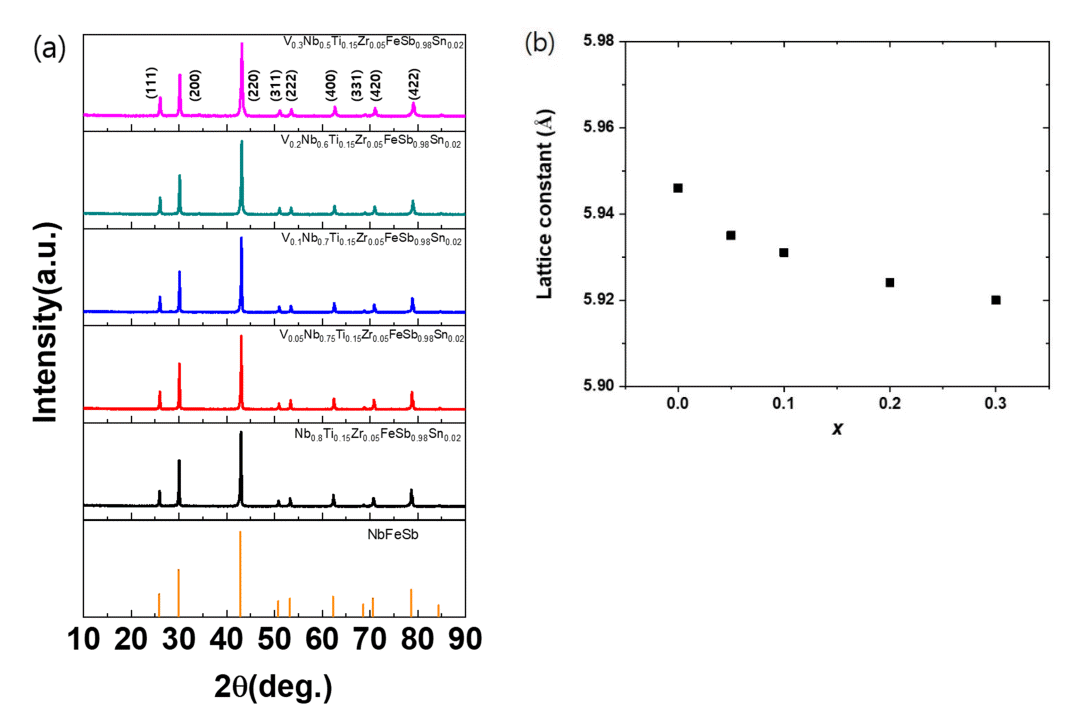
(a) X-ray diffraction patterns and (b) lattice constants of the Nb0.8−xVxTi0.15Zr0.05FeSb0.98Sn0.02 (x = 0, 0.05, 0.1, 0.2, and 0.3) samples.
Figures 2(a)–(e) show the microscopic morphology of the fractured surfaces of the Nb0.8−xVxTi0.15Zr0.05FeSb0.98Sn0.02 samples, which were observed using FE-SEM. Large grains with diameters of >10 μm are mixed with small grains, and all samples exhibit various grain sizes. EBSD was used for a more detailed microstructural analysis, and Figures 2(f) and 2(g) show the inverse pole figure image along the [001] direction and the grain map of the Nb0.7V0.1Ti0.15Zr0.05FeSb0.98Sn0.02 sample, respectively. The random distribution of the [001] pole and the wide-ranging grain sizes are visible in these results, from which the statistical data presented in Figure 2(h) were extracted. The data indicate that the average grain size is unrelated to the V content and the standard deviation is large in all the samples. In addition, two-dimensional maps of the constituent elements, which are not shown in this study, confirmed that the materials are homogeneous.
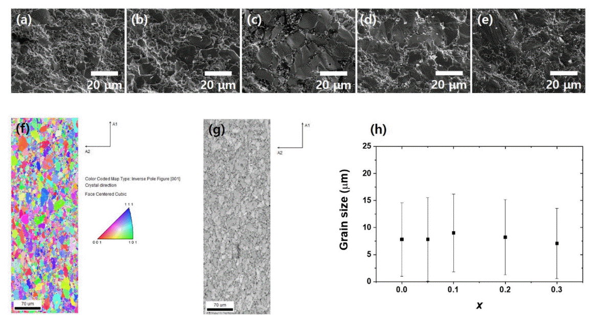
(a)–(e) FE-SEM images of the fractured surfaces of the Nb0.8–xVxTi0.15Zr0.05FeSb0.98Sn0.02 (x = 0, 0.05, 0.1, 0.2, and 0.3) samples, respectively. (f) Inverse pole figure image obtained along the [001] direction, and (g) grain map of the Nb0.7V0.1Ti0.15Zr0.05FeSb0.98Sn0.02 sample. (h) Graph of the average grain size of the Nb0.8−xVxTi0.15Zr0.05FeSb0.98Sn0.02 samples versus the V content, which was extracted statistically using the EBSD analysis.
Figure 3(a) shows the σ of the Nb0.8−xVxTi0.15Zr0.05FeSb0.98Sn0.02 samples over the temperature range of 298–973 K. The samples demonstrate a metallic conduction behavior in which electrical conductivity decreases with increasing temperature. The σ vs. T data points are well fitted with several exponential curves following the T−n law, where the exponent n decreases from 1.30 (x = 0) to 0.78 (x = 0.3) as the V content increases. This behavior indicates that the carrier scattering mechanism changes gradually from acoustic phonon dominated to mixed scattering, reflecting the increasing effect of alloy scattering with the addition of V [12,13,15,21]. Figure 3(b) shows the plots of the carrier concentration and mobility at 300 K as functions of the V content. The carrier concentration of the V-free sample is 3.3 × 1021 cm−3, and it decreases monotonically to 1.7 × 1021 cm−3 at x = 0.3, with a similar trend in carrier mobility.
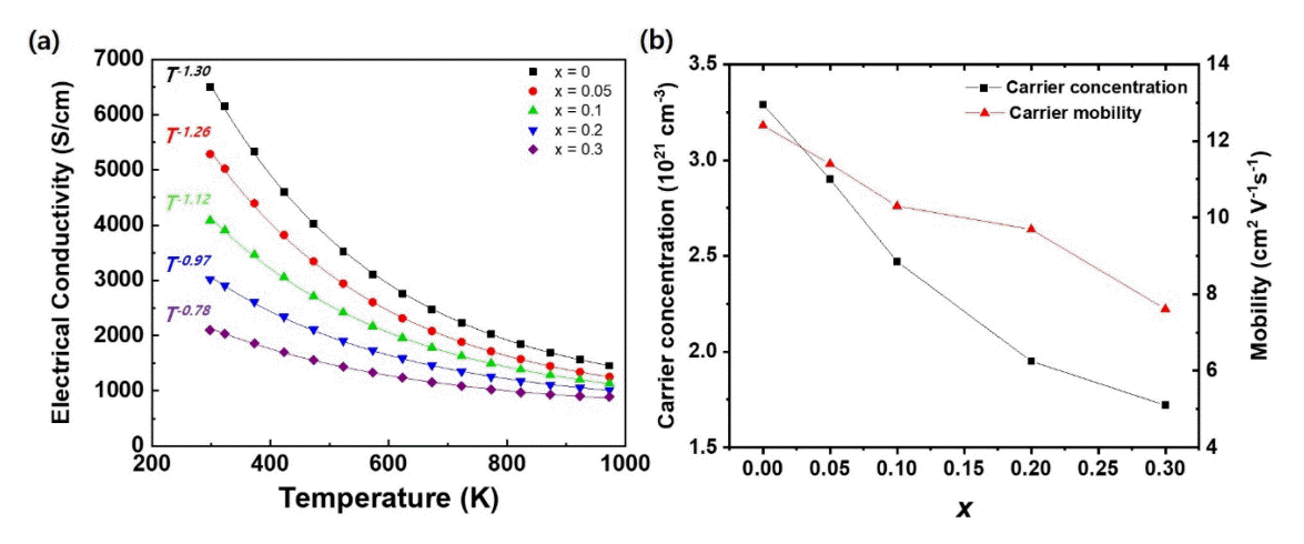
(a) Temperature dependence of electrical conductivity, and (b) carrier concentration and mobility versus x of the Nb0.8−xVxTi0.15Zr0.05FeSb0.98Sn0.02 (x = 0, 0.05, 0.1, 0.2, and 0.3) samples.
The decreasing carrier concentration with increasing V content can be understood based on previous reports showing that pure VFeSb is n type [22,23] and a certain amount of Ti is required to transform n-type VFeSb into a p-type material [22-25]. Thus, a part of the p-type dopants is consumed for compensation in VFeSb, which lowers the concentration of active dopants available to produce the major carriers, i.e., holes. Furthermore, the reduced solubility and doping efficiency of the Zr and Ti dopants with increasing V content has been reported to be one of the origins of the decreasing carrier concentration [26]. The reduction in carrier mobility with the addition of V is attributed to the combined effect of alloy scattering {Figure 3(a)} and the larger band effective mass of the hole in VFeSb versus in NbFeSb [11,26].
Figure 4(a) presents a comparison of the S of the Nb0.8−xVxTi0.15Zr0.05FeSb0.98Sn0.02 samples from 298 to 973 K. Overall, S increases with x over the entire temperature range when x ≤ 0.1. The maximum S (Smax) was observed at the highest measurement temperature of 973 K, reaching 186.7 μV K−1 in the sample with x = 0.1. However, as x increases further, Smax decreases and shows a maximum value at <973 K, as observed at x = 0.3. This is because VFeSb has a narrower bandgap (Eg) than NbFeSb [11,22,23], which is related to Smax according to the approximate equation |Smax | » Eg /(2eTmax) [27]. Here, Tmax is the temperature at which |S| is maximized. As Eg decreases with the addition of V, the excitation of thermally activated minority carriers across the bandgap is promoted at low temperatures. Consequently, bipolar conduction becomes non-negligible, causing |S| to saturate and begin to decrease at low temperatures.

Temperature dependence of the (a) Seebeck coefficient and (b) power factor of the Nb0.8−xVxTi0.15Zr0.05FeSb0.98Sn0.02 (x = 0, 0.05, 0.1, 0.2, and 0.3) samples.
Figure 4(b) shows the power factor (PF) calculated using the formula PF = σS2. The V-free sample has the highest PF, and almost constant values of 4.85–4.90 mW m−1K−2 are obtained in the temperature range of 523–773 K. By comparison, the V-added samples show increasingly smaller values of PF as the V content increases, due to the reduced σ. The decrease in PFmax is inversely proportional to x and reduces by ~37% at x = 0.3. These results suggest that the substitution of Nb with V is not advantageous in terms of PF.
Meanwhile, Figure 5(a) clearly indicates that the addition of V reduces thermal conductivity. Thermal conductivity (κ) decreases with temperature in all the samples, and the maximum κ (κmax) is observed at 298 K. The κmax of the V-free sample is ~10.1 W K−1 m−1. However, adding a small V content causes a considerable decrease in κmax, as seen in the Nb0.75V0.05Ti0.15Zr0.05FeSb0.98Sn0.02v sample, whose κmax was reduced by ~17.5% to a value of 8.33 W K−1 m−1. A more dramatic reduction in κmax was observed in the V-rich samples, and the κmax value of the Nb0.5V0.3Ti0.15Zr0.05FeSb0.98Sn0.02 sample was reduced by more than 50% to ~4.93 W K−1 m−1 by V alloying. Notably, κ comprises three components— contributions from the lattice (κlat), majority carrier (κel), and bipolar conduction (κbi). Therefore, an independent estimation of each component is required to establish a fair comparison of the κlat values of the samples.

Temperature dependence of (a) thermal conductivity and (b) lattice thermal conductivity of the Nb0.8−xVxTi0.15Zr0.05FeSb0.98Sn0.02 (x = 0, 0.05, 0.1, 0.2, and 0.3) samples.
First, κbi can be ignored considering the extremely high majority carrier concentrations {Figure 3(b)}, and κel is calculated by applying the Wiedemann–Franz law:
where L denotes the Lorenz number. When a single parabolic band model is assumed, the S and Lorenz number are calculated using Fermi–Dirac integrals Fn(ξ) as follows [28]:
where r and ξ denote the scattering parameters and the reduced Fermi energy, EF/kT, respectively. We calculated L and then subtracted the calculated κel to obtain the lattice thermal conductivity, κlat, as shown in Figure 5(b). The dependence of κlat on temperature is the same as that of κ shown in Figure 5(a); however, κlat decreases with increasing V content until x = 0.2, above which κlat remains almost unchanged. In the Nb0.6V0.2Ti0.15Zr0.05FeSb0.98Sn0.02 sample, the κmax at 298 K decreased by ~36% compared with the κmax of the V-free sample, whereas the difference between the κlat values decreases at higher temperatures.
Figure 6 shows zT and summarizes the total effects of V addition. Based on the results of this study, the samples with x < 0.1 had a higher zTs than those of the V-free sample over the entire temperature range. The maximum zT value of 0.89 was observed in the Nb0.75V0.05Ti0.15Zr0.05FeSb0.98Sn0.02v and Nb0.7V0.1Ti0.15Zr0.05FeSb0.98Sn0.02 samples at 973 K, which is ~5% higher than that of the V-free Nb0.8Ti0.15Zr0.05FeSb0.98Sn0.02 sample. Although the improvement is insignificant, we believe that a small V content can still be used to fine-tune NbFeSb-based thermoelectric materials.
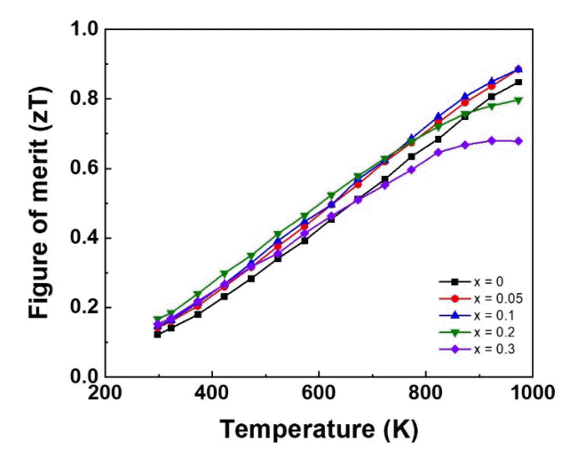
Temperature dependence of zT for the Nb0.8−xVxTi0.15Zr0.05FeSb0.98Sn0.02 (x = 0, 0.05, 0.1, 0.2, and 0.3) samples.
4. CONCLUSIONS
The effect of V alloying on TEP was investigated in this study using Hf-free HH alloys Nb0.8−xVxTi0.15Zr0.05FeSb0.98Sn0.02 (x = 0, 0.05, 0.1, 0.2, and 0.3). The carrier concentration and mobility reduced when V was substituted for Nb, and the lattice thermal conductivity decreased substantially even with a small V content. Notably, the addition of V reduces κlat even when the materials are already codoped with Ti, Zr, and Sn, which effectively function as phonon scattering centers. Furthermore, a maximum zT value of 0.89 was obtained for Nb0.75V0.05Ti0.15Zr0.05Sn0.98Sb0.02 at 973 K by adding V.
Acknowledgements
This research was supported by the Korea Electrotechnology Research Institute Primary research program through the National Research Council of Science & Technology (NST), which is funded by the Ministry of Science and ICT (MSIT) (Code number 22A01023).
Notes
Conflict of Interest
The authors have no conflicts of interest to declare.