


1. INTRODUCTION
There is growing social demand for energy-harvesting technologies that utilize ambient mechanical energy resources. Moreover, much research on self-powered wearable electronics based on human motion is ongoing [1]. Developing piezoelectric materials that simultaneously exhibit excellent piezoelectricity and flexibility is important work. Traditional piezoelectric materials are represented by perovskite ceramics such as Pb(Zr,Ti)O3 and BaTiO3 due to their large piezoelectric coefficients [2]. Because these ceramics are brittle, they are incorporated into the polymers such as PDMS, PVDF, and PMMA in the form of nanomaterials for application to wearable devices [3,4]. Therefore, a comprehensive understanding of the synthesis and characterization of piezoelectric nanomaterials is important.
The characterization of piezoelectric nanomaterials is particularly important for a couple of reasons. First, the properties of piezoelectric materials, such as piezoelectric coefficients and aging properties, are governed by the domain structures [5,6]. Our understanding of the domain structures and their switching behaviors in bulk materials has been improved over the last decade with advances in modelling [7-10] and characterization techniques [11]. However, these domain structures in nanomaterials differ from those in bulk materials due to the different synthesis processes and sizes. Furthermore, certain characterization techniques for bulk materials are not suitable for nanomaterials due to their size differences. To control and manipulate nanomaterials precisely, delicate characterization techniques are essential.
Since atomic force microscopy (AFM) was invented by Gerd Binnig in 1986 [12], AFM has been applied to diverse research areas, including physics, chemistry, materials science and mechanical engineering [13-15]. Imaging topographic features at the nanometer scale used to be the primary use of AFM. However, diverse AFM-based characterization techniques have been developed, taking advantage of the physical interactions between the AFM tip and the sample surfaces. Representative AFM-based characterization techniques include piezoresponse force microscopy (PFM) [16], conductive AFM (C-AFM) [17], Kelvin probe force microscopy (KPFM) [18] and scanning capacitance microscopy (SCM) [19]. Particularly, the radius of a commercial AFM tip is approximately 20 nm, enabling precise control of nanomaterials. Therefore, AFM is irreplaceable for characterizing the diverse functional properties of nanomaterials.
This review paper focuses on the use of AFM for the electromechanical characterization of piezoelectric and ferroelectric nanomaterials. First, three AFM-based characterization techniques (PFM, C-AFM, and lateral force microscopy (LFM)) often used for piezoelectric nanomaterials are introduced. While PFM works based on the converse piezoelectric effect to image piezoelectric domain structures, C-AFM measures the current induced by the direct piezoelectric effect in nanomaterials. Finally, LFM is widely used for evaluating the mechanical properties of nanomaterials. Thereafter, previous studies of the application of these techniques to piezoelectric and ferroelectric nanomaterials are discussed in detail.
2. AFM-BASED ELECTROMECHANICAL CHARACTERIZATION TECHNIQUES
2.1 Piezoresponse force microscopy
Prior to introducing the working principle of PFM, it is worthy to introduce direct and converse piezoelectric effects. Direct effect is the phenomenon in which polarization is generated by externally applied stress. Meanwhile, in converse effect strain is induced by externally applied electric field. These two effects can be described by the following two equations.
where D is the polarization, d is the piezoelectric coefficients, T is the stress, ε is the dielectric constant, E is the electric field, S is the strain, and s is the material compliance. It is noted that the superscript T and E mean a zero or constant stress and electric field, respectively [2].
PFM works by exciting local converse piezoelectric responses on sample surfaces when AC voltage is applied to an AFM probe [16]. The resulting surface displacement vector consists of vertical and lateral components. In the vertical PFM mode, the vertical motion of an AFM cantilever is monitored using a position-sensitive photodetector and a lock-in amplifier. Depending on the polarization direction in the sample, the relationship between the externally applied AC voltage signal and the resulting surface displacement signal is either in-phase or out-of-phase. It should be noted that a domain is a region in which a single electric polarization direction is defined. Based on this working principle, distinct domains can be discriminated. This is the basic working principle of imaging ferroelectric domain structures using PFM. Unlike the resonant frequency in tapping mode, multiple contact resonant frequencies are present in PFM. When PFM works near one of these contact resonant frequencies, the cantilever oscillation amplitude is significantly enhanced [20,21]. This enhanced cantilever oscillation enables one to resolve ferroelectric domain structures on the nanometer scale [22,23].
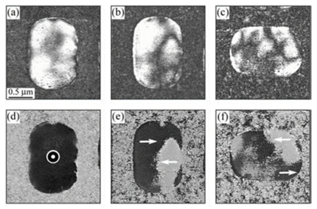
Vertical and lateral PFM signals can be acquired during PFM measurements. Occasionally, it is difficult to discriminate multiple domains with similar polarization directions using only vertical PFM. When the vertical components of displacement vectors originating from two distinct domains are very similar, it can be difficult to distinguish the two domains using vertical PFM phase and amplitude signals. In this case, the lateral components of PFM signals provide important information about the polarization directions. Lateral PFM signals are either positive or negative depending on the torsional behavior of the cantilever induced by the lateral component of surface displacement vector. Thus, lateral PFM signals change as the sample is rotated. Based on this principle, a three-dimensional PFM technique composed of one vertical and two orthogonal lateral PFM images has been used to construct a three-dimensional map of the polarization directions [24-26]. Fig 1 shows the three-dimensional PFM phase and amplitude images for a Pb(Zr,Ti)O3 capacitor [25]. Although the vertical PFM phase image (Fig 1(d)) shows a single domain, multiple domains can be observed from the two orthogonal lateral PFM phase images (Figs 1(e)‒(f)).
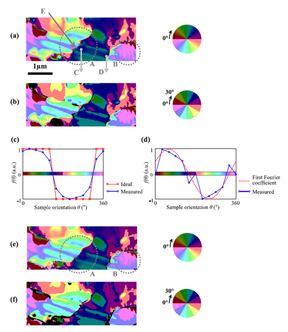
However, multiple domains with similar polarization directions are still challenging to discriminate using the three-dimensional PFM method. In this case, the angle-resolved PFM method can often provide a viable solution (Fig 2). The local surface displacement vector induced by the converse piezoelectric effect rotates with the rotation of the sample such that the lateral PFM phase signal passes through 0 during a 360° sample rotation, as shown in Figs 2(c)‒(d). By monitoring the rotation angle at which the phase signal changes from positive to negative, or vice versa, a map of the angle-resolved PFM can be generated [27-29]. Fig 2(a) and 2(b) differ from Fig 2(e) and (f) in that Fig 2(a) and 2(b) were generated using PFM signals from 0 ° ≤θ≤180 ° and Fig 2(e) and (f) from 180 ° ≤θ≤360 ° . In addition, the AR-PFM maps were generated using the first Fourier coefficient(Fig 2(a),(e)) and the rotation segment method(Fig 2(b),(f)). From these AR-PFM images, non-180 ° domain structures with a curvy 180 ° (marked by E in Fig 2(a)) can be clearly observed by various color codes. Furthermore, as the same domains are represented by the same color code, the AR-PFM maps provide more intuitive information that is difficult to expect from conventional PFM techniques.
Meanwhile, the conventional PFM excites and detects the piezoelectric response at a single frequency via a lock-in amplifier. As mentioned earlier, by selecting the frequency at the contact resonant frequency, the amplitude of the piezoelectric response can be significantly enhanced. However, important information such as energy transfer data during PFM measurements is dependent on the driving frequency. To overcome this issue, well-calibrated PFM techniques such as a dual-frequency resonance-tracking method [30] and a band excitation method [31] have been invented. Finally, for a quantitative understanding of the local-domain switching behavior, switching spectroscopy PFM (SS-PFM) has been used [32]. Using this technique, a range of important material properties, such as imprints and hysteresis loops, can be quantitative analyzed. Additionally, local domain switching can be conducted by applying DC bias to the sample surface through the AFM tip [33].
As introduced earlier, PFM works by exciting the local surface displacement in the sample surface. However, when voltage is applied to the sample surface via an AFM probe, there are several possible mechanisms such as electrochemical strain, electrochemical dipoles, charge injection/field effect, and Joule heating contributing to the surface displacement. For example, in electrochemical (Vegard) strain mechanism surface displacement occurs via ionic motion which can be induced by the voltage applied to the AFM probe. In highly conductive material surfaces, local thermal expansion can take place when current flows, which is called Joule heating, also affecting measuring surface displacements. For these reasons, PFM signals can be observed even from non-ferroelectric materials although converse piezoelectric effect cannot be induced in these materials. Numerous attempts have been made to decouple piezoelectric effect from non-piezoelectric effects, and some novel techniques including contact Kelvin probe force microscopy have been developed to tackle this issue [34,35].
2.2 Conductive atomic force microscopy
The working principle of C-AFM is relatively simple compared to that of PFM. The metal-coated AFM tip serves as a movable top electrode, and the sample is connected to the bottom electrode. Electric bias is applied either to the AFM probe or the bottom electrode, generating an electric potential difference across the sample thickness. Consequently, current flows through the interior of the sample, and a preamplifier converts the current into voltage.
The measured current (I) in C-AFM can be represented as
where J and Aeff are the current density and the effective emission area, respectively [17]. In this case, Aeff should be particularly distinguished from the physical contact area between the AFM tip and the sample surface when the AFM tip is directly in contact with the electrically conductive sample area. Additionally, Aeff corresponds to the electrically conductive local area.
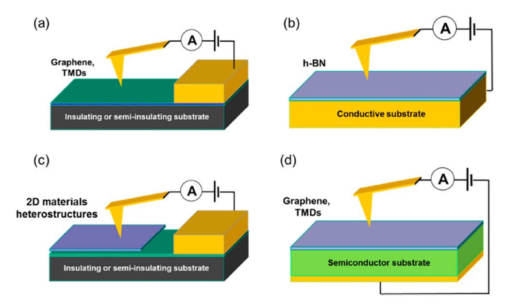
C-AFM can be used to measure the in-plane current as well as the out-of-plane current through certain designs of the material and position of the bottom electrode. To enable inplane current measurements, an insulating material should be used for the bottom substrate, while a patterned electrode must to be formed on top of the bottom substrate [36]. The arrangement and material selection for the substrate are particularly important when C-AFM is used to characterize two-dimensional materials such as transition-metal dichalcogenides (TMDs) and graphene [37]. Depending on the specific designs, various types of measurements, such as lateral (or vertical) current transport, tunneling current, and current injection measurements, can be realized by C-AFM, as shown in Fig 3.
When a current map for the area of a certain sample is produced by C-AFM, constant tip bias or substrate bias is used. However, C-AFM can be used without an external voltage source when the AFM probe scans a piezoelectric nanomaterial. If the material is sufficiently small and soft enough to induce strain using the AFM probe, piezoelectric potential is internally generated via a direct piezoelectric effect [38]. This will be discussed in detail in section 3.2.
Since the birth of C-AFM by M. P. Murrel in 1993 [39], it has become one of the most important techniques for characterizing the local electrical properties of materials. Particularly, C-AFM is irreplaceable for characterizing electrical properties in thin dielectrics, as dielectric degradation is induced by local defects [40-44]. For instance, the local electrical conductivity in thin dielectrics is influenced by structural inhomogeneities, including those at the grain boundary [42,44], and these can be observed through topographic features. Readers can refer to a review article in the literature [45] about the application of C-AFM to dielectrics. Finally, C-AFM has been preferentially used to probe the electrical properties of one-dimensional nanomaterials such as carbon nanotubes and germanium nanowire due to its excellent lateral resolutions [46,47].
2.3 Lateral force microscopy
When the fast scan direction is oriented perpendicular to the cantilever, torsion in the AFM probe is induced by the friction force between the AFM tip and the sample surface. LFM works by monitoring the torsional behavior of the AFM probe through a laser beam reflected off the cantilever onto a position-sensitive photodetector consisting of four sectors. The standard operation of AFM in contact mode is suitable for studying the force of friction in that the set point in the feedback system corresponds to the degree of cantilever deflection. Thus, the normal force applied to the sample surface by the AFM tip and consequently the force of kinetic friction can be precisely controlled by the set point.
LFM, also known as friction force microscopy (FFM), was invented in 1987 by Mate et al. to evaluate the atomic-scale friction between a tungsten tip and the basal plane of a graphite surface [48]. The use of LFM has risen with the growing interest in friction force measurements on the nanometer scale. Understanding nanotribology is a prerequisite for designing micro- and nanoelectromechanical systems (MEMS and NEMS) [49-51]. Nanotribology includes the factors of friction, wear, surface roughness, and adhesion, and a comprehensive understanding of these multiple effects is required. For instance, the force of friction on the micro- or nanometer scale originates from material-induced and topography-induced effects. A topography-induced effect can be distinguished from a material-induced effect by comparing LFM signals during trace and retrace scans [52].
LFM can also be an effective tool when studying micro- and nanomechanics, as a tiny object can be precisely manipulated by an AFM probe. For instance, LFM has been exploited to measure the force of friction between two silica particles [53] as well as the force of adhesion between tungsten nanoparticles and a flat gold surface [54]. Particularly, LFM is an effective method for measuring the elastic modulus of nanowires. This will be discussed in detail in section 3.3.
In LFM, there are two major issues to be solved for an accurate measurement of frictional forces. The first issue is the coupling between normal force and lateral force channels, which has several causes. The second issue is to find an accurate lateral force constant [55]. Finding a lateral force constant through a mathematical model is difficult because the dimensions of AFM probes differ from one another. For this reason, numerous efforts have been made to calibrate lateral forces properly [56]. Various methods have been employed for calibrating LFM. These can be grouped into approaches that rely on optical geometry [57], pivot and mirror tilting [58], and a horizontal lever [59].
3. APPLICATION OF AFM-BASED CHARACTERIZATION TECHNIQUES TO PIEZOELECTRIC AND FERROELECTRIC NANOMATERIALS
3.1 Characterization of nanomaterials using piezoresponse force microscopy
We can classify the existing literature associated with imaging ferroelectric domains in nanowires into two groups based on the positions of the nanowires, i.e., whether they lie on the substrate or whether they are free-standing nanowires. First, PFM has been used to confirm piezoelectricity in numerous piezoelectric nanowires lying on a substrate, including BaTiO3 [60], Pb(Zr,Ti)O3 [61], GaN [62], (K,Na)NbO3 [63], and BiFeO3 [64]. Using the SS-PFM method, the local hysteresis behavior of the piezoelectric response of a single BiFeO3 nanowire has been observed [64]. PFM can be exploited for more quantitate evaluations with regard to the piezoelectric properties of nanowires. For instance, approximate piezoelectric coefficients can be obtained from locally measured piezoelectric response signals [62,65]. The use of a tiny AFM tip provides a great advantage to those studying local piezoelectric properties within a single nanowire. By combining vertical and lateral PFM methods, the dependency of the polarization switching behavior on the axial and transverse directions of nanowire can be identified [60].
Quantitative measurement techniques such as SS-PFM can provide important clues related to novel nanowire materials. For example, the piezoelectric properties of a (K,Na)NbO3 nanowire can be enhanced by finding the composition corresponding to the specific phase boundary [63]. For various (K,Na)NbO3 nanowires with different K/Na ratios, local switching behaviors were studied using SS-PFM. The maximum piezoelectric response was observed at a ratio of approximately 45/55 K/Na. More reliable data for piezoelectric coefficients can be obtained using well-calibrated PFM techniques. For instance, to examine the enhanced piezoelectric responses of PbTiO3 and Pb(Ti,Zr)O3 nanowires with self-sustained negative pressure, a dual AC resonance tracking method was exploited [66]. As indicated in Fig 4, the local piezoelectric responses of a single PbTiO3 nanowire can be precisely probed.
Given that PFM works in contact mode, it requires very careful measurement skills to image domain structures in free-standing nanorods. Nevertheless, SS-PFM operates similarly to the force-volume mode, and for this reason PFM has been applied to various free-standing nanorods, including KNbO3 [67], InGaAs [68], and BaTiO3 nanowires [69], to measure local piezoelectric responses. To locate the AFM tip precisely on the free-standing BaTiO3 nanorod, topography images are acquired in tapping mode, as shown in Fig 5(a) [69]. Thereafter, local piezoelectric switching behavior can be observed in a specific nanorod.
Meanwhile, although C-AFM has been preferentially used to evaluate the piezoelectric performance capabilities of individual ZnO nanorods, PFM provides rich information about the piezoelectric properties of ZnO nanorods. For instance, the piezoelectric responses and the polarity of ZnO nanorods can be examined by PFM [70]. Because ZnO simultaneously exhibits piezoelectric and semiconducting properties, the free charge carrier concentration due to intrinsic defects and impurities can increase to 1020 (cm-3). In this case, the piezoelectric properties of individual nanorods could significantly differ due to differences in charge carrier concentrations.
Meanwhile, nanofibers fabricated by an electrospinning process are applicable to flexible electrodes, sensors and fillers in composite materials [71]. A typical electrospinning process is composed of a high-voltage power supply, a syringe, and a grounded nanofiber collector. When sufficiently high voltage is applied to molten polymer at the tip of the syringe, a charged jet of fluid is ejected from the tip of the syringe. While the molten polymer travels from the syringe to the collector through the air, the solvent is evaporated. There are several review papers of electrospinning techniques [72-74].
A PFM-based analysis of piezoelectric properties has been conducted with diverse nanofibers such as BaTiO3 [75], Pb(Zr0.3,Ti0.7)O3 [76], BiFeO3 [77], a BaTiO3/PVDF composite [78], PVDF with silver decorated multiwall CNTs [79], Fe3O4/PVDF [80], and PVDF nanofibers [81]. PFM has been exploited to confirm piezoelectricity in novel materials such as a BaTiO3/PVDF composite nanofiber [78]. Using PFM phase and amplitude images, it was found that the central region of the BaTiO3/PVDF composite nanofiber exhibits domains with opposite polarizations compared to the remaining regions. Given the size of the nanofibers, the AFM tip on the nanometer scale is essential to identify the local effective piezoelectric coefficients of nanofibers. For example, the d33 value of Pb(Zr0.3,Ti0.7)O3 nanofibers was measured and found to be 83.4 pmV-1 [76]. For PVDF nanofibers, the measured d33 values differed depending on the location, and the d33 value in the periphery region exceeded that in the central parts [81]. The amplitude of piezoelectric response signals in PVDF/Fe3O4 nanofiber were similar along the length but very different among different nanofibers [80].
Well-calibrated PFM techniques enrich an analysis of the piezoelectric properties of a single PVDF nanofiber. For instance, vertical and lateral PFM measurements of a PVDF nanofiber using a dual AC resonance tracking technique showed that the out-of-plane piezoelectric response exceeded the in-plane piezoelectric response [82]. Additionally, a quantitative analysis of local switching behavior using SSPFM showed that the piezoelectric coefficient d33 is dependent on the diameter of the PVDF nanofibers.
The use of PFM is not constrained to measuring electromechanical properties but can also be extended to measuring mechanical properties such as the Young’s modulus of nanofibers [83]. PFM has been used to evaluate the mechanical properties of the Pb(Zr0.52Ti0.48)O3-CoFe2O4 composite nanofiber, showing that the Young’s modulus increased and the piezoelectric response decreased with an increase in the CoFe2O4 content. In this work, mechanical and piezoelectric properties were simultaneously mapped, taking advantage of the contact resonance of the cantilever and theoretical models.
3.2 Characterization of nanomaterials using conductive atomic force microscopy
Piezoelectric nanowires or nanorods have drawn attention since the first C-AFM study of vertically grown ZnO nanorods by Wang and Song in 2006 [38]. Figs 6(a) and (b) show the topography and C-AFM images of vertically grown n-type ZnO nanorods obtained during C-AFM measurements, respectively. C-AFM operates in contact mode, and the set point in the feedback circuit is the normal force exerted by the AFM tip on the sample surface. Due to the finite response time of the feedback circuit, the AFM probe deflects ZnO nanorods, generating piezoelectric potential. When the metal-coated AFM tip is in contact with the compressed side of the n-type ZnO nanorod, a Schottky barrier is formed, generating electric current. Fig 6(d) shows that current signal is detected from the C-AFM measurement when the AFM tip is in contact with the compressed side of an n-type ZnO nanorod.
Because ZnO simultaneously exhibits piezoelectric and semiconducting properties, a flow of charge carriers by the piezoelectric potential is readily induced [84]. Meanwhile, a ZnO nanorod doped with phosphorous exhibits p-type semiconducting properties [85]. When C-AFM measurements were taken on a p-type ZnO nanorod using the AFM tip coated with Pt, the current signal was detected when the AFM tip touched the stretched side of the ZnO nanorod.
Since the pioneering work on ZnO nanorods using C-AFM, studies of the other piezoelectric nanowires with wurtzite structures such as CdS [86], ZnS [87], InN [88], GaN [89,90] and CdSe [91] have been carried out. In these works, the AFM tip was used to deflect vertically grown nanowires and to measure the current generated by the piezoelectric potential. The piezoelectric coefficients of materials with wurtzite structures tend to be smaller than those of materials with a perovskite structure such as Pb(Zr,Ti)O3 and BaTiO3 . Thus, the misunderstanding that a larger current signal should be detected from Pb(Zr,Ti)O3 nanowires is common. However, actual C-AFM measurements of Pb(Zr,Ti)O3 nanowires have shown the opposite result [92]. It was found that even if the piezoelectric coefficient of a Pb(Zr,Ti)O3 nanowire is large, the resultant C-AFM signal can be similar to that of ZnO nanowires due to the high dielectric constant of Pb(Zr,Ti)O3 .
By conducting C-AFM measurements of ZnO nanorods, useful information for enhancing the power generation efficiency of a piezoelectric nanogenerator can be obtained. For instance, when an AFM tip coated with a nitrogen-doped diamond material was used for C-AFM measurements on n-type ZnO nanorod, current signals were detected from a large number of ZnO nanorods [93]. This occurred because when the nitrogen-doped diamond was in contact with the n-type ZnO, a rectifying n+‒n heterojunction formed. This result indicates the importance of proper materials selection for electrodes in piezoelectric nanogenerators based on n-type ZnO nanorods. Meanwhile, for nanogenerators based on vertically grown piezoelectric nanorods, the morphology of the nanowires plays an important role. The growth directions of piezoelectric nanowires are typically vertical but are subjected to compressive force in the normal direction. For this reason, the piezoelectric performance can be affected by obliquely aligned piezoelectric nanorods. In this case, the piezoelectric effect of an obliquely aligned individual nanorod can be precisely evaluated by the C-AFM technique [94]. The optimal sizes of ZnO nanorods controlled by the growth methods [95] or the growth time [96] for application to piezoelectric nanogenerators can also be evaluated by C-AFM. Meanwhile, the piezoelectric performance capabilities of nanogenerators can be enhanced via a chemical doping approach. For instance, the enhanced piezoelectric potential of ZnO nanorods by Cr doping was evaluated using C-AFM [97]. In GaN nanowire, the density of free charge carriers can be controlled by Si doping [98]. As shown in Fig 7, the optimal doping level in GaN nanowires for application to a piezoelectric nanogenerator was evaluated using C-AFM measurements.
Finally, the current-voltage characteristics of ZnO nanorods can be observed while applying an external force to the nanorods via an AFM probe. Fig 8(a) shows ZnO nanorods grown via a vapor-liquid-solid process on a GaN/sapphire substrate using Au nanoparticle catalysts [99]. While applying compressive stress to the ZnO nanorods via the AFM probe, the current-voltage characteristics were studied using C-AFM. The result showed that the current flowing through the nanorods can be controlled by the normal force applied to the nanorods (Figs 8(c)‒(d)). This effect can be explained by the piezoelectric tuning effect of the Schottky barrier at the Au-ZnO junction.
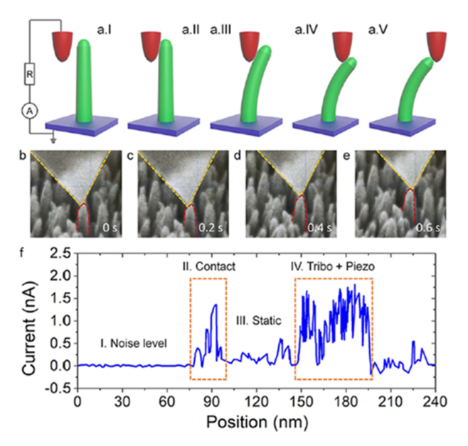
As mentioned earlier, it has been believed since the initial report that the current measured from ZnO nanorods by C-AFM originates from the piezoelectric effect of the ZnO nanorods [38]. Since then, it has been taken for granted that only the piezoelectric effect is responsible for the C-AFM signals from ZnO nanorods. However, this misconception was corrected by recent work in which the interaction between the AFM tip and ZnO nanorods was monitored in situ via a scanning electron microscope during C-AFM measurements [100]. This work showed that the contact potential and triboelectric effect along with the piezoelectric effect are responsible for current signals generated during C-AFM measurements on ZnO nanorods (see Fig 9). Fig 9(a.I–V) illustrate the deflecting process of the ZnO nanorod using the AFM probe. This process was precisely observed using a C-AFM intergrated into an SEM (Fig 9(b)-(e)). As can be seen from Fig 9(f), considerable current signals were detected when the AFM probe touched or was in contact with the stretched side of n-type ZnO nanorods, indicating that the current did not originate from piezoelectric effect.
3.3 Characterization of nanomaterials using lateral force microscopy
Piezoelectric nanowires or nanorods are subjected to external mechanical forces when they are integrated into piezoelectric devices. Thus, accurately measuring the mechanical properties of piezoelectric nanowires is important for their application to piezoelectric devices. One of the earliest attempts to measure the elastic modulus of piezoelectric nanowire was on vertically grown ZnO nanowires [101]. In this study, while deflecting ZnO nanowires with the AFM tip, the elastic modulus was estimated based on the LFM signals. To compute the elastic modulus, topography and lateral force signals were used as important data. To improve the precision of the mechanical test for a single ZnO nanowire, a nanowire clamped in a trench pattern was deflected by means of AFM lateral manipulations [102]. Using this method, Wen et al. found that the Young’s modulus is not dependent on diameter but on the ultimate strength, can be significantly enhanced for nanowires with small diameters. A creative experimental arrangement was designed by Jiang et al. to measure the shear modulus of ZnO nanorods [103]. In this work, a ZnO nanorod was horizontally placed along the edge of a Si trench, after which one end of the nanorod was fixed to the trench side wall. While the AFM tip scans the reclined ZnO nanorod, the shear deformation and lateral force are monitored through topography and LFM signals, respectively.
Although this review is focused on piezoelectric nanomaterials, it is important here to introduce a few more works on the mechanical testing on non-piezoelectric nanowires using LFM. One of the earliest attempts at a mechanical test of a single nanowire was conducted by Wu et al. in 2005 [104]. In this work, an Au nanowire was suspended on a trench and the two ends of the nanowire were clamped. Bending of the nanowire was executed by loading lateral force using an AFM tip. It was found that the Young’s modulus is not dependent on the diameter of the Au nanowire but on the yield strength, which increases as the diameter decreases. A similar experimental setup was employed to study the elastic properties of Si nanowires, and LFM was used to measure the magnitude of the force applied to the nanowire [105] (see Fig 10).
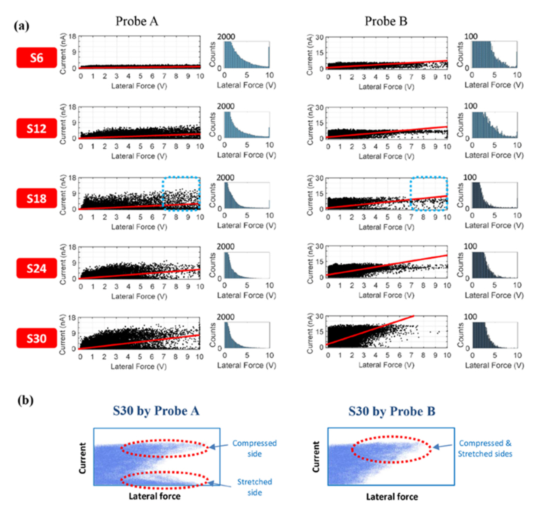
Thus far, previous studies that undertook evaluations of piezoelectric nanomaterials using PFM, C-AFM, and LFM have been introduced. The piezoelectricity of a ZnO nanorod was discovered for the first time via a comparative analysis of C-AFM and topography signals. Likewise, AFM-based measurements of piezoelectric nanomaterials can be clarified via a comparative analysis of multiple signals. For example, for vertically aligned ZnO nanorods, it was clarified that both piezoelectric and triboelectric effects are responsible for the current signals through the simultaneous acquisition of C-AFM and LFM signals [106]. For five ZnO nanorods with different aspect ratios, C-AFM and LFM signals were simultaneously acquired and the resultant two sets of signals were statistically analyzed. In this work, two AFM probes with different spring constants were used to identify the effects of normal force on the experimental result. As shown in Fig 11(b), depending on the spring constant of the AFM probe and the normal force applied to the AFM probe, scatter plots of the current versus lateral force showed different patterns. When n-type ZnO nanorods were deflected by the AFM probe with a small spring constant(Probe A), large lateral force with no current could be generated when the AFM probe was in contact with the stretched side of the ZnO nanorods. Contrarily, when they were deflected by the AFM probe with a large spring constant(Probe B), the data points corresponding to the large lateral force with no current vanished. It was elucidated that a considerable amount of current could originate from the triboelectric effect induced by friction between the AFM tip and a ZnO nanorod when the normal force applied to the AFM probe is large.
4. CONCLUSION
This article has reviewed the application of AFM-based electromechanical characterization techniques to piezoelectric and ferroelectric nanomaterials. Owing to the small tip size of the AFM probe, the piezoelectric properties of nanomaterials can be locally measured using PFM. Over the last decade, PFM techniques have significantly advanced, and more quantitative analysis outcomes of the piezoelectric properties for nanowires, nanorods, and nanofibers can be realized with the dual-frequency resonance tracking method and SS-PFM.
Compared to PFM, the use of C-AFM for piezoelectric nanomaterials has been somewhat monotonous because the measurement process of C-AFM does not require dynamic motion of the cantilever. The primary use of C-AFM has been to confirm piezoelectricity from vertically grown piezoelectric nanorods. C-AFM can also be applied indirectly to evaluate the performance of piezoelectric devices by observing the effects of the nanorod size, the coating material of the AFM tip, and the alignment of nanorods on the resultant current signals. With these advances in microscopic techniques, it was elucidated that C-AFM signals can originate from the contact potential, triboelectric effect as well as the piezoelectric effect.
The mechanical properties of individual piezoelectric nanowires have been evaluated using LFM. For accurate measurements, a single nanowire was suspended on a trench and then deflected by the AFM tip using a programmed-manipulation path. Based on measured lateral force signals, the mechanical properties of nanowires, specifically the elastic modulus and ultimate strength, have been measured. Our understanding the physical interaction between the AFM tip and the nanorod during the C-AFM measurement process was improved by simultaneously monitoring both C-AFM and LFM signals. With the excellent adaptability of AFM and the rapidly advancing microscopic techniques, there is no doubt that AFM-based characterization techniques will be central to the measurements of the electromechanical properties of piezoelectric and ferroelectric nanomaterials.