


1. INTRODUCTION
Thermoelectric materials are used to generate power and for solid-state cooling by exploiting their ability to convert heat into electricity (Seebeck effect) and heat pumping with electricity (Peltier effect). The energy conversion efficiency of thermoelectric devices is primarily determined by the dimensionless figure of merit, ZT = ╬▒2Žā╬║-1T, where Z is the temperature-dependent figure of merit, T is the absolute temperature, ╬▒ is the Seebeck coefficient, Žā is the electrical conductivity, and ╬║ is the thermal conductivity [1-3]. Cu-based chalcogenides, which are composed of low-toxicity, low-cost, and earth-abundant elements, are considered promising p-type thermoelectric materials because of their excellent thermoelectric performance [3, 4]. The ternary Cu-Sb-S sulfide system comprises four major phases: CuSbS2 (chalcostibite), Cu12Sb4S13 (tetrahedrite), Cu3SbS3 (skinnerite), and Cu3SbS4 (famatinite). Famatinite crystallizes in an ordered zinc-blende superstructure with space group I4 ┬»
Because the thermoelectric performance of pure Cu3SbS4 is mainly limited by low electrical conductivity caused by the low carrier concentration, approaches have been studied to optimize the carrier concentration by partially substituting (doping) other elements for Cu or Sb. Shen et al. [15] reported a ZT of 0.76 at 623 K for Cu3Sb0.89Bi0.06Sn0.05S4 by co-doping Bi and Sn at the Sb sites. Suzumura et al. [16] obtained a ZT of 0.095 at 323 K for Cu2.91Ag0.09Sb0.98Ge0.02S4 by co-doping Ag at the Cu and Ge at the Sb sites. Chen et al. [17] reported ZT values of 0.37 at 523 K for Cu2.25Ni0.75SbS4 and 0.22 at 523 K for Cu3Ni0.05Sb0.95S4 by substituting Ni into the Cu and Sb sites, respectively. Tanishita et al. [18] achieved a ZT of 0.67 at 623 K for Cu3Sb0.75Ge0.1P0.15S4 by co-doping Ge and P at Sb sites. Pi et al. [19] reported a ZT of 0.67 at 623 K for Cu3Sb0.92Sn0.08S4 by substituting Sn at Sb sites. In our previous study [20], In-doped famatinite was successfully fabricated through mechanical alloying (MA) and hot pressing (HP), and Cu3Sb0.94In0.06S4 exhibited a ZT of 0.16 at 623 K. Although the improvement in thermoelectric performance by single doping with In was small, by double doping famatinite with Sn and In, the ZT value was expected to increase in this study due to additional lattice scattering and enhanced electrical properties (electrical conductivity and power factor). The Cu3Sb1-x-ySnxInyS4 compounds were prepared by partially introducing Sn and In at the Sb sites via the MA-HP process. A phase/microstructural analysis was conducted, and the thermoelectric properties were examined.
2. EXPERIMENTAL
Sn and In double-doped famatinites, Cu3Sb1-x-ySnxInyS4 (x = 0.02, 0.04, 0.08, 0.10, 0.12, and y = 0.06, 0.08, 0.10), were prepared using MA and HP methods to prevent volatilization of the component elements and for homogeneous synthesis. Powders of Cu (purity 99.9%, <45 ╬╝m), Sb (purity 99.999%, <150 ╬╝m), Sn (purity 99.999%, <35 ╬╝m), In (purity 99.99%, <75 ╬╝m), and S (purity 99.99%, <75 ╬╝m) were used to prepare stoichiometric compositions. The starting powder was loaded into a stainless-steel jar with stainless-steel balls. The jar was evacuated and sealed with Ar gas, and then MA was performed for 12 h at a rotation speed of 350 rpm using a planetary ball mill (Pulverisette5, Fritsch). The synthesized powder was charged into a graphite mold and consolidated using HP at 70 MPa and 623 K for 2 h in vacuum.
The phases present in the MA-HP specimens were analyzed using an X-ray diffractometer (XRD; D8-Advance, Bruker) with Cu K╬▒ radiation. The diffraction peaks were measured over a 2╬Ė (diffraction angle) range of 10┬░ to 90┬░ in steps of 0.02┬░. The lattice constants were estimated using TOPAS, a Rietveld refinement program. The microstructures of the sintered specimens were observed using a scanning electron microscope (SEM; Quanta400, FEI) in the backscattering electron (BSE) mode. Composition analysis and elemental mapping were conducted using an energy-dispersive spectrometer (EDS; Quantax200, Bruker), where the energy levels of the elements employed were the Cu K series, Sb L series, Sn L series, In L series, and S K series. The charge transport parameters were measured using the van der Pauw method (Keithley 7065).
Rectangular bars of 3.5 ├Ś 3.5 ├Ś 10 mm3 were processed from sintered bodies for Seebeck coefficient and electrical conductivity measurements, which were performed using the DC four-probe method with the ZEM-3 system (Advance Riko) in a He atmosphere. To determine thermal conductivity, the thermal diffusivity, specific heat, and density were measured in a vacuum using the laser flash method with TC-9000H equipment (Advance Riko) on specimens cut into disks with a diameter of 10 mm and a thickness of 1 mm. Finally, the power factor and ZT values were calculated from the electrical conductivity, Seebeck coefficient, and thermal conductivity.
3. RESULTS AND DISCUSSION
Figure 1 shows the XRD results for Cu3Sb1-x-ySnxInyS4 produced by the MA-HP process. All the samples contained the tetragonal famatinite phase (ICDD PDF# 00-035-0581); however, a secondary phase of CuInS2 was identified in specimens with y = 0.10. The calculated lattice constants and relative densities are listed in Table 1. In previous studies the lattice constants of undoped Cu3SbS4 have been reported to be 0.5384 nm (a-axis) and 1.0749 nm (c-axis) [19]; however, in this study, Sn/In double doping increased the a-axis to 0.5387ŌĆō0.5389 nm and changed the c-axis to 1.0744ŌĆō1.0752 nm. Pi et al [19] reported that by doping Sn in Cu3Sb1-xSnxS4 (x = 0.02ŌĆō0.10), the lattice constant of the a-axis slightly decreased from 0.5384 nm to 0.5377ŌĆō0.5379 nm, but the c-axis increased significantly from 1.0749 nm to 1.0775ŌĆō1.0778 nm. In our previous study [20], when In was doped into Cu3Sb1-yInyS4 (y = 0.02ŌĆō0.08), the a-axis was slightly reduced from 0.5384 nm to 0.5377ŌĆō0.5380 nm, but the c-axis was greatly increased from 1.0749 nm to 1.0781ŌĆō1.0791 nm.
However, in the present study, double doping with both Sn and In at the Sb sites in famatinite yielded changes in the lattice constants unlike those produced by single doping with Sn or In. The reason for this is still uncertain, but it is presumed that the tetragonality of famatinite was changed by the Sn/In double doping. The effect of double doping on the lattice constants of famatinite has not previously been reported.
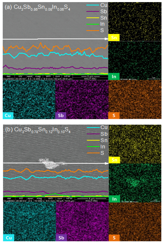
Figure 2 shows the BSE-SEM images with elemental line scans and maps of Cu3Sb0.86Sn0.08In0.06S4 and Cu3Sb0.78Sn0.12In0.10S4. As confirmed by the XRD results in Fig 1, Cu3Sb0.86Sn0.08In0.06S4 (Fig 2(a)) appeared as a single famatinite phase, and all elements were uniformly distributed. However, Cu3Sb0.78Sn0.12In0.10S4 (Fig 2(b)) contained a secondary phase with a higher In content and lower Sb content than the matrix (famatinite), and from the XRD phase analysis shown in Fig 1, this was estimated to be the CuInS2 phase. All specimens exhibited densely sintered bodies with relative densities of 96.1%ŌĆō97.8% (Table 1) of the theoretical density (4.64 g cm-3) of Cu3SbS4 [21]. Changes in the theoretical density arising from the doping contents of Sn and In were not considered.
The charge transport parameters of Cu3Sb1-x-ySnxInyS4 are presented in Table 1. All the samples had positive Hall coefficients, indicating p-type semiconductors whose major charge carriers were holes (not indicated in Table 1). As the Sn and In contents increased from Cu3Sb0.90Sn0.04In0.06S4 to Cu3Sb0.80Sn0.12In0.08S4, the carrier (hole) concentration increased from 1.12 ├Ś 1019 to 1.72 ├Ś 1019cm-3, and the mobility also increased from 111 to 307 cm2V-1s-1. Chen et al. [9] reported that the carrier concentration of Cu3SbS4 was 3.2 ├Ś 1017cm-3 and increased to 7.8 ├Ś 1019ŌĆō1.0 ├Ś 1021cm-3 for Cu3Sb1-xSnxS4 (x = 0.01ŌĆō0.15). Goto et al. [22] reported that with increasing Sn content for Cu3Sb1-xSnxS4 (x = 0ŌĆō 0.15), the carrier concentration increased from 4.2 ├Ś 1018 to 7.8 ├Ś 1020 cm-3. Shen et al. [15] reported that as the Sn content of Cu3Sb0.94-xBi0.06SnxS4 (x = 0.01ŌĆō0.09) increased, the carrier concentration increased to 9.3 ├Ś 1019ŌĆō7.4 ├Ś 1020 cm-3. Tanishita et al. [18] reported that the carrier concentration of Cu3SbS4 was 1.5 ├Ś 1017 cm-3, and that of Cu3Sb0.85-xGexP0.15S4 (x = 0.05ŌĆō0.4) increased to 0.5 ├Ś 1021ŌĆō2.3 ├Ś 1021 cm-3 as the Ge content increased.
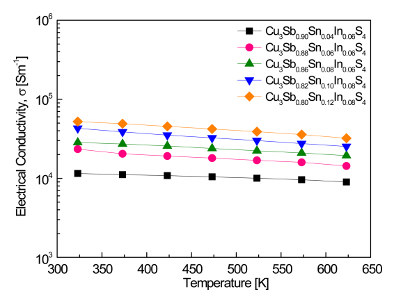
Figure 3 shows the electrical conductivity of Cu3Sb1-x-ySnxInyS4. The electrical conductivity of a heavily doped semiconductor is defined as Žā = en╬╝, where e is the electronic charge, n is the carrier concentration, and ╬╝ is the carrier mobility [23]. In this study, all the samples exhibited degenerate semiconductor behavior, where the electrical conductivity slightly decreased as the temperature increased. When the In content was constant at y = 0.06, as the Sn content increased from x = 0.04 to 0.08, the electrical conductivity increased from 1.2 ├Ś 104ŌĆō9.0 ├Ś 103 S m-1 to 2.8 ├Ś 104ŌĆō1.9 ├Ś 104 S m-1 at 323ŌĆō623 K. These values are significantly higher than those (2.6 ├Ś 102ŌĆō1.1 ├Ś 103 S m-1 at 323ŌĆō623 K) reported in our previous study [20]. As the Sn and In contents further increased, as can be seen in Table 1, the carrier concentration and mobility increased, and thus the electrical conductivity increased, with Cu3Sb0.80Sn0.12In0.08S4 having the highest electrical conductivity of 5.2 ├Ś 104ŌĆō3.2 ├Ś 104 S m-1 at 323ŌĆō623 K. Chen et al. [9] reported that the electrical conductivity of undoped Cu3SbS4 was 89 S m-1 at 300 K, and that as the Sn content of Cu3Sb1ŌłÆxSnxS4 (x = 0.01ŌĆō0.15) increased, the electrical conductivity increased to 6.7 ├Ś 103ŌĆō1.3 ├Ś 105 S m-1. Pi et al. [19] reported that the electrical conductivity of Cu3SbS4 was 57ŌĆō490 S m-1 at 323ŌĆō623 K, but that as the Sn content of Cu3Sb1ŌłÆxSnxS4 (x = 0.02ŌĆō 0.10) increased, it increased to 4.0 ├Ś 103ŌĆō3.7 ├Ś 104 S m-1 at 323 K and to 4.2 ├Ś 103ŌĆō2.3 ├Ś 104 S m-1 at 623 K. Shen et al. [15] reported that as the Bi and Sn contents of Cu3Sb1-x-yBixSnyS4 (x = 0.02ŌĆō0.14 and y = 0.01ŌĆō0.09) increased, the electrical conductivity increased, achieving a maximum electrical conductivity of 9.4 ├Ś 104 S m-1 at 300 K for Cu3Sb0.85Bi0.06Sn0.09S4. In the present study, the electrical conductivity had lower values compared to the reported values, in accordance with the lower carrier concentrations.
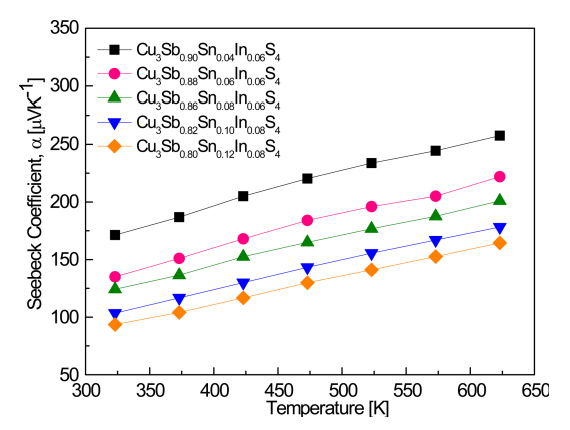
Figure 4 shows the Seebeck coefficients of Cu3Sb1-x-ySnxInyS4. All the samples exhibited positive Seebeck coefficients, similar to the signs of the Hall coefficient, confirming that they were p-type semiconductors. The Seebeck coefficient is simply expressed as ╬▒ = Cm*Tn-2/3 using the Pisarenko relationship [24], where C is a constant and m* is the effective carrier mass. The Seebeck coefficient increased as the temperature increased, in contrast to the temperature dependence of the electrical conductivity [25], and decreased as the Sn and In contents increased, because it has an inverse relationship with carrier concentration. The value of the Seebeck coefficient was 171ŌĆō258 ╬╝V K-1 at 323ŌĆō623 K for Cu3Sb0.90Sn0.04In0.06S4, but decreased to 124ŌĆō201 ╬╝V K-1 for Cu3Sb0.86Sn0.08In0.06S4 and to 94ŌĆō164 ╬╝V K-1 for Cu3Sb0.80Sn0.12In0.08S4.
Chen et al. [9] reported that the Seebeck coefficient of Cu3SbS4 was 670 ╬╝V K-1 at 300 K, and for Cu3Sb1-xSnxS4 (x = 0.01ŌĆō0.15), the carrier concentration increased with increasing Sn content, resulting in a decreased Seebeck coefficient of 264ŌĆō72 ╬╝V K-1. Pi et al. [19] reported that the Seebeck coefficient of Cu3SbS4 was 575ŌĆō539 ╬╝V K-1 at 323ŌĆō623 K, and for Cu3Sb1-xSnxS4 (x = 0.02ŌĆō0.10), it decreased from 260ŌĆō338 ╬╝V K-1 for Cu3Sb0.98Sn0.02S4 to 118ŌĆō197 ╬╝V K-1 for Cu3Sb0.90Sn0.10S4. In our previous study [20], the Seebeck coefficient of Cu3Sb1-yInyS4 (y = 0.02ŌĆō0.08) decreased as the In content increased: 499ŌĆō488 ╬╝V K-1 for Cu3Sb0.98In0.02S4 and 336ŌĆō404 ╬╝V K-1 for Cu3Sb0.92In0.08S4 at 323ŌĆō623 K. Compared with the previous study, a significant decrease in the Seebeck coefficient was confirmed to have resulted from the double doping with Sn and In. Shen et al. [15] obtained lower Seebeck coefficients of 352ŌĆō95 ╬╝V K-1 at 300 K for Bi/Sn-double-doped Cu3Sb0.94-xBi0.06SnxS4 (x = 0.01ŌĆō0.09).
Figure 5 shows the power factors of Cu3Sb1-x-ySnxInyS4. The power factor is expressed as PF = ╬▒2Žā. Optimized carrier concentration is required to achieve a high power factor because it is affected by both the Seebeck coefficient, which is inversely proportional to the carrier concentration, and the electrical conductivity, which is proportional to the carrier concentration. The power factor of Cu3SbS4 reported by Pi et al. [19] was 0.02ŌĆō0.14 mW m-1 K-2 at 323ŌĆō623 K, and in our previous study [20] on Cu3Sb1-yInyS4 (y = 0.02ŌĆō0.08), Cu3Sb0.94In0.06S4 exhibited the highest power factor of 0.03ŌĆō0.18 mW m-1 K-2 at 323ŌĆō623 K, implying that the improvement in the power factor caused by In single doping was not significant.
However, in this study, the power factor was remarkably increased by the Sn and In double doping; it increased to 0.44ŌĆō0.78 mW m-1 K-2 at 323ŌĆō623 K for Cu3Sb0.86Sn0.08In0.06S4, with Cu3Sb0.80Sn0.12In0.08S4 exhibiting the highest power factor of 0.46ŌĆō0.87 mW m-1 K-2. Pi et al. [19] reported that for Cu3Sb1-xSnxS4 (x = 0.02ŌĆō0.10), Cu3Sb0.92Sn0.08S4 had the highest power factor, 0.94 mW m-1 K-2 at 623 K, as a result of the trade-off relationship between electrical conductivity and Seebeck coefficient. Shen et al. [15] reported that for Cu3Sb0.94-xBi0.06SnxS4 (x = 0.01ŌĆō0.09), Cu3Sb0.85Bi0.06Sn0.09S4 had the highest power factor of 1.40 mW m-1 K-2 at 623 K, a result of carrier concentration optimization caused by the Bi and Sn double doping. In the present study, the Seebeck coefficient of Cu3Sb0.80Sn0.12In0.08S4 was similar to that of Cu3Sb0.85Bi0.06Sn0.09S4 reported by Shen et al. [15], but its electrical conductivity was approximately half as great; thus, the power factor led to a lower value.
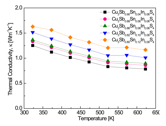
Figure 6 shows the thermal conductivity of Cu3Sb1-x-ySnxInyS4. In the temperature range 323ŌĆō623 K, the thermal conductivity decreased as the temperature increased, and a bipolar effect did not occur. In our previous study [20], the thermal conductivity of Cu3Sb0.94In0.06S4 was 1.20ŌĆō0.68 W m-1 K-1 at 323ŌĆō623 K, but in the present study, the thermal conductivity increased with increasing Sn and In contents: 1.37ŌĆō0.90 W m-1 K-1 for Cu3Sb0.86Sn0.08In0.06S4 and 1.63ŌĆō1.17 W m-1 K-1 for Cu3Sb0.80Sn0.12In0.08S4 at 323ŌĆō623 K. Pi et al. [19] reported that the thermal conductivity of Cu3SbS4 was 1.14ŌĆō0.62 W m-1 K-1 in the temperature range 323ŌĆō623 K and increased when Sn was doped, so that for Cu3Sb1-xSnxS4 (x = 0.02ŌĆō0.10), the thermal conductivity was 1.26ŌĆō0.72 W m-1 K-1 for Cu3Sb0.98Sn0.02S4 and 1.32ŌĆō0.88 W m-1 K-1 for Cu3Sb0.90Sn0.10S4. Shen et al. [15] reported that the thermal conductivity of Cu3Sb0.94-xBi0.06SnxS4 (x = 0.01ŌĆō0.09) increased to 1.74ŌĆō2.28 W m-1 K-1 at room temperature as the Sn content increased from x = 0.01 to 0.09 as a result of the increase in electronic thermal conductivity, and for samples with Sn content lower than x = 0.05, the thermal conductivity was lower than that of Cu3Sb0.94Bi0.06S4. In this study, it was also confirmed that the electronic thermal conductivity contributed significantly to the increase in thermal conductivity due to Sn/In double doping.
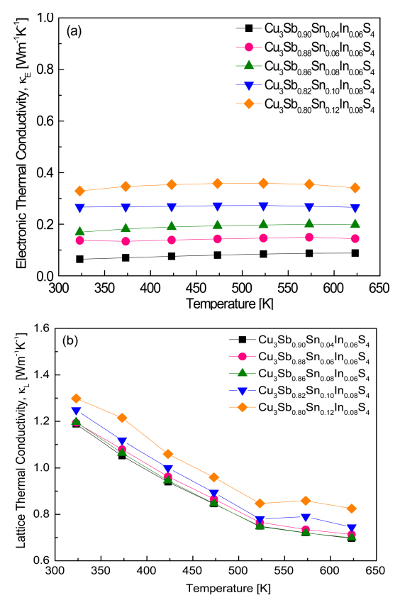
Figure 7 shows (a) the electronic thermal conductivity (╬║E) of the carriers and (b) the lattice thermal conductivity (╬║L) of the phonons for Cu3Sb1-x-ySnxInyS4. The Wiedemann-Franz law (╬║E = LŽāT) was employed to estimate the electronic thermal conductivity, where L is the Lorenz number [26]. The Lorenz number [10-8 V2 K-2] can be obtained using the relation L = 1.5 + exp(ŌĆō|╬▒|/116) [27,28], and the calculated values are listed in Table 1. As illustrated in Fig 7 (a), the electronic thermal conductivity was not significantly affected by temperature, but it increased as the electrical conductivity and Lorenz number increased with increasing Sn and In contents. Thus, over the temperature range 323ŌĆō623 K, the electronic thermal conductivity of Cu3Sb0.90Sn0.04In0.06S4 increased from 0.06 to 0.09 W m-1 K-1, that of Cu3Sb0.86Sn0.08In0.06S4 from 0.17 to 0.20 W m-1 K-1, and that of Cu3Sb0.80Sn0.12In0.08S4 from 0.33 to 0.34 W m-1 K-1. Pi et al. [19] reported that, over the same temperature range, the electronic thermal conductivity of Cu3SbS4 increased from 0.27 ├Ś 10-3 to 0.40 ├Ś 10-2 W m-1 K-1, and that of Cu3Sb1-xSnxS4 (x = 0.02ŌĆō0.10) increased from 0.27 ├Ś 10-3ŌĆō0.40 ├Ś 10-2 W m-1 K-1 at 323 K to 0.04ŌĆō0.23 W m-1 K-1 at 623 K. In our previous study [20], the electronic thermal conductivity of Cu3Sb1-yInyS4 (y = 0.02ŌĆō0.08) was 0.42 ├Ś 10-3ŌĆō0.13 ├Ś 10-2 W m-1 K-1 at 323 K and 0.58 ├Ś 10-2ŌĆō0.10 W m-1 K-1 at 623 K. The electronic thermal conductivity was higher than that of undoped Cu3SbS4 because of the increase in carrier concentration caused by the dopants.
Figure 7 (b) shows the lattice thermal conductivity of Cu3Sb1-x-ySnxInyS4, which is the value obtained by subtracting the electronic thermal conductivity from the total thermal conductivity. The lattice thermal conductivity decreased as the temperature increased, resulting from the Umklapp scattering caused by acoustic phonons (╬║L is in fact directly proportional to T-1) [29]. In our previous study [20], the lattice thermal conductivity of Cu3Sb0.94In0.06S4 was 1.20ŌĆō0.67 W m-1 K-1 at 323ŌĆō623 K, which was higher than the values 1.15ŌĆō0.62 Wm-1K-1 for Cu3SbS4 reported by Pi et al. [19]. In the present study, Cu3Sb0.90Sn0.04In0.06S4 showed the lowest lattice thermal conductivity of 1.19ŌĆō0.70 W m-1 K-1 at 323ŌĆō623 K. When the In content was y = 0.06, there was no significant change in the lattice thermal conductivity with increasing Sn content. However, when the Sn and In contents were further increased, the lattice thermal conductivity slightly increased, and for Cu3Sb0.80Sn0.12In0.08S4, the lattice thermal conductivity was 1.30ŌĆō0.83 W m-1 K-1 at 323ŌĆō623 K. This is thought to be due to the formation of a secondary phase, such as CuInS2, beyond the solubility limit of Sn and In at the Sb site of famatinite. Pi et al. [19] reported that the lattice thermal conductivity of Cu3Sb1-xSnxS4 (x = 0.02ŌĆō0.10) was 1.24ŌĆō1.10 W m-1 K-1 at 323 K and 0.68ŌĆō0.64 W m-1 K-1 at 623 K. Shen et al. [15] reported that the lattice thermal conductivity of Cu3Sb0.94-xBi0.06SnxS4 (x = 0.01ŌĆō0.09) was 1.69ŌĆō1.83 W m-1 K-1 at 300 K and decreased to 0.75 W m-1 K-1 as the temperature increased to 623 K.
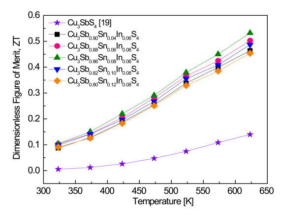
Values of the dimensionless figure of merit ZT of Cu3Sb1-x-ySnxInyS4 are presented in Fig 8. In the temperature range 323ŌĆō623 K, the ZT values increased with increasing temperature. This was because intrinsic conduction and bipolar effects did not occur in the measurement temperature range [30]. Compared with the ZT values of 0.14 at 623 K for Cu3SbS4 [19] and 0.16 at 623 K for Cu3Sb0.94In0.06S4 [20], Cu3Sb0.86Sn0.08In0.06S4 exhibited an improved ZT value of 0.53 at 623 K, resulting from the significantly increased power factor caused by double-doping with Sn and In. Although the highest power factor was achieved in Cu3Sb0.86Sn0.12In0.08S4, this sample exhibited the relatively low ZT value of 0.45 at 623 K, because of its high thermal conductivity. Goto et al. [12] fabricated Cu3SbS4 and Cu3Sb0.85Sn0.15S4 via anvil pressing of powders synthesized by the melting-annealing method and obtained ZT values at 623 K of 0.03 and 0.1, respectively. Chen et al. [31] reported that Cu3SbS4 and Cu3Sb0.95Sn0.05S4 produced by the MA-SPS (spark plasma sintering) process exhibited ZT values at 623 K of 0.1 and 0.72, respectively. Shen et al. [15] prepared Cu3Sb0.89Bi0.06Sn0.05S4 by the MA-SPS process and obtained a ZT of 0.76 at 623 K. Tanishita et al. [18] reported that Cu3Sb0.75Ge0.1P0.15S4 produced by HP after synthesis using melting-annealing exhibited a ZT of 0.67 at 623 K, this value being due to an increase in carrier concentration from the Ge doping and a decrease in lattice thermal conductivity from the P doping.
4. CONCLUSIONS
Cu3Sb1-x-ySnxInyS4 (x = 0.02ŌĆō0.12 and y = 0.06ŌĆō0.10) famatinites double-doped with Sn and In were synthesized and sintered by MA-HP. According to the XRD and SEM analyses, a single famatinite phase was obtained in all samples, except for the sample with y = 0.10, in which a secondary phase of CuInS2 was found. By double-doping with Sn and In at the Sb sites of famatinite, the lattice constant of the a-axis was slightly increased from 0.5384 nm to 0.5387ŌĆō0.5389 nm, while the lattice constant of the c-axis changed from 1.0749 nm to 1.0744ŌĆō1.0752 nm. Sn/In-double-doped famatinites were confirmed to be p-type semiconductors by their positive Hall and Seebeck coefficients. The temperature dependence of the electrical conductivity and Seebeck coefficient followed degenerate semiconductor behavior. The carrier concentration increased with increasing Sn and In contents, and thus, the electrical conductivity increased, and the Seebeck coefficient decreased. Cu3Sb0.80Sn0.12In0.08S4 exhibited the highest power factor of 0.87 mW m-1 K-2 at 623 K. However, Cu3Sb0.86Sn0.08In0.06S4 reached the highest ZT value of 0.53 at 623 K because of a high power factor of 0.78 mW m-1 K-2 and low thermal conductivity of 0.90 W m-1 K-1.